Figures & data
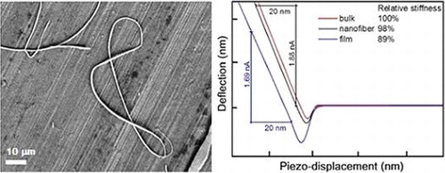
Figure 1. (a) Photo of the As-S glass electrospinning experimental setup (b) Photography shows a As-S glass nanofiber layer electrospun for 10 min on Al foil substrate with the diameter of the layer ~15 cm. (c) Images show layers spun for 1, 2 and 10 min. The right-hand side of the samples were coated with a 3 nm thin Au layer after the electrospinning (Color online).
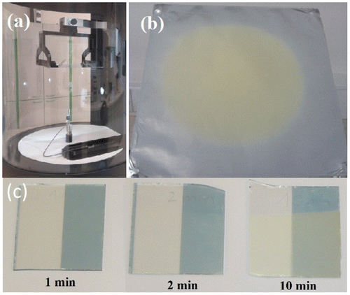
Figure 2. SEM micrographs of the chalcogenide As-S glass isolated nanofibers and nanofiber layers prepared by electrospinning of the glass solution on Al foil substrate. The spinning times were (a) and (b) 1 min, (c)–(f) 20 min for stationary, parts (a)–(c), (e), and rotating, parts (d) and (f) collectors.
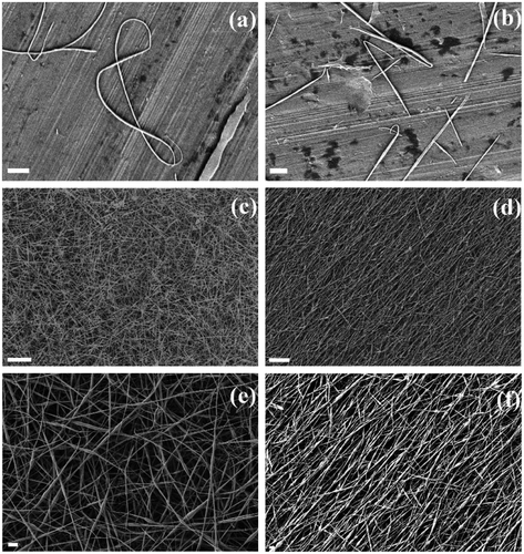
Figure 3. (a) Optical transmittance spectra of chalcogenide As3S7 glass aligned or unaligned nanofibrous layers after 1, 2 and 10-min deposition onto the silica glass slides substrates coated with ITO/FTO are shown in comparison with of 100 nm and 2 μm spin-coated layer onto a microscope slide, and the bulk glass. (b) Optical transmittance spectra of the chalcogenide As3S7 glass nanofibrous layers after 1, 2 5 and 10 min of deposition are shown in comparison with the same layers coated with a 3 nm layer of gold and a 3 nm single-layer of gold f.
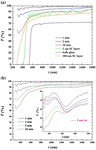
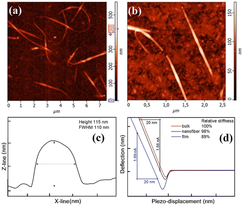
Figure 4. (a) and (b) AFM topography of chalcogenide As3S7 glass nanofibers deposited for 2 min. (c) The profile recorded from the nanofiber shown in part (b). (d) The dependence of the tip deflection on the piezo-displacement; the region of the repulsive interactions is used to compare the relative stiffness of the As3S7 bulk glass, the well-annealed spin-coated film and the electrospun chalcogenide nanofiber (Color online).