Figures & data
Figure 1. Ge–Sb–Se ternary diagram with the two selected compositions (GeSe2)90(Sb2Se3)10 (Ge28.1Sb6.3Se65.6, Se2) and (GeSe2)50(Sb2Se3)50 (Ge12.5Sb25Se62.5, Se6) for the bulk glass targets and the sputtered films.
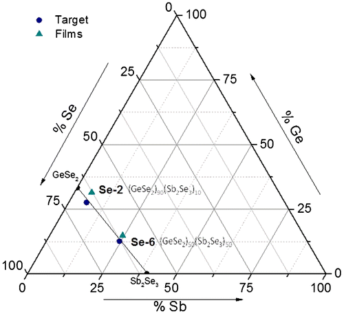
Figure 2. Chemical composition of (GeSe2)90(Sb2Se3)10 (Ge28.1Sb6.3Se65.6, Se2) and (GeSe2)50(Sb2Se3)50 (Ge12.5Sb25Se62.5, Se6) sputtered films and bulk glass targets determined by EDS analysis (±1 at.%) compared to theoretical composition.
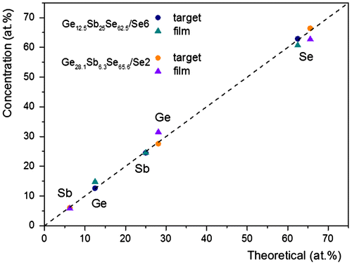
Figure 3. Refractive index in near- and mid-IR (±0·01) extracted from VASE data of bulk targets and sputtered (Ge28.1Sb6.3Se65.6, Se2) and (Ge12.5Sb25Se62.5, Se6) thin films.
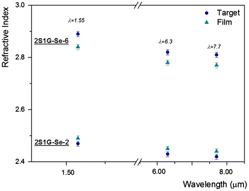
Figure 4. (a) SEM image of guiding (Ge12.5Sb25Se62.5, Se6) and cladding (Ge28.1Sb6.3Se65.6, Se2) sputtered layer of mid-IR structure, (b) dispersion curves of refractive indices (±0·01) of the sputtered layers, estimated by the analysis of VASE data via Sellmeier model.
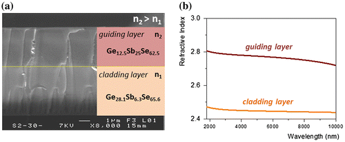
Figure 5. (a) Scheme and (b) SEM image of cross-section of chalcogenide ridge waveguide, (c) fundamental mode TM00 intensity profile for the optimal geometrical parameters (width w and height h) of chalcogenide waveguide and evolution of the evanescent power factor η as a function of w, h for single-mode propagation in the detection of any substance dissolved at λ = 7·66 μm.
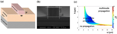
Figure 6. (a) Near field of propagated light at λ = 7·7 μm and microscopic image of single-mode ridge waveguides in S-shape configuration. (b) Optical propagation loss at λ = 7·7 μm measured by mode profile imaging method for selenide ridge waveguides with height equal to 1·7 μm and width of 10 μm. Each point represents averaged data for 3 experimental measures.
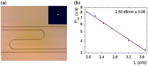
Figure 7. (a) Mid-IR absorbance spectra of toluene at 100 v/v % and water at T = 278 K. (b) Power transmitted response as a function of the waveguide length taking into consideration the strong absorbance of water in the mid-IR. (c) Scheme of waveguide functionalization: a polymer non-absorbing in the mid-IR is deposited as superstrate for detection of pollutants dissolved in water.
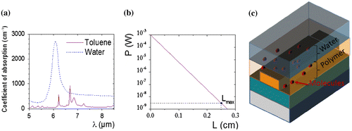
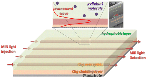
Figure 8. Scheme of a mid-IR sensor constituted of a selenide buffer (Ge28.1Sb6.3Se65.6, Se2) and a ridge selenide waveguide (Ge12.5Sb25Se62.5, Se6) coated with a polymer allowing molecules detection by evanescent wave spectroscopy.