
Figures & data
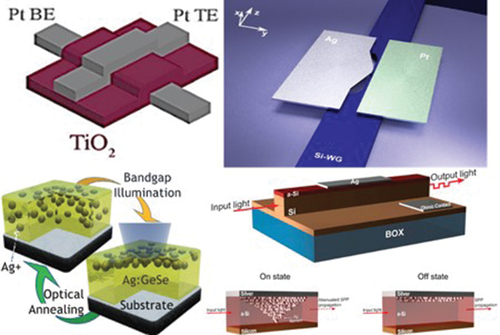
Figure 1. Factors influencing material utilization in ionic-based devices (a) the melting point (Tm) and self-diffusion activation energy (Q) of various elements commonly used in ionic devices are grouped into three categories denoted by green, blue, and red loops. Li is used as a reference element due to its high mobility ion and established presence in ionic batteries (Ref. [Citation42]). (b) Standard potential (determines the tendency of elements to oxidation “red” or reduction “blue”) of most common metals (W, Ta, Mo, Nb, Hf, Pt, Ni, Pd, Ti, Cu, Ag, Au, Al) utilized in ionic devices as well as Si as a well-known substrate material in intrinsic or nitride form and sometimes solid electrolyte in oxide form (SiO2) (Ref [Citation43]).
![Figure 1. Factors influencing material utilization in ionic-based devices (a) the melting point (Tm) and self-diffusion activation energy (Q) of various elements commonly used in ionic devices are grouped into three categories denoted by green, blue, and red loops. Li is used as a reference element due to its high mobility ion and established presence in ionic batteries (Ref. [Citation42]). (b) Standard potential (determines the tendency of elements to oxidation “red” or reduction “blue”) of most common metals (W, Ta, Mo, Nb, Hf, Pt, Ni, Pd, Ti, Cu, Ag, Au, Al) utilized in ionic devices as well as Si as a well-known substrate material in intrinsic or nitride form and sometimes solid electrolyte in oxide form (SiO2) (Ref [Citation43]).](/cms/asset/1c642427-7f06-4565-bf18-e2494a8ee834/tapx_a_2338285_f0001_oc.jpg)
Figure 2. Optical constants of well-known metals (Au, Ag, Al, Cu, Pt, Pd, Ni) in ionic-based switching devices. (a) Refractive indices, (b) Extinction coefficients, (c), (d) Real and imaginary permittivity components (ϵ1, ϵ2). (e), (f) SPP and LSPR FOM of these metals (Ref. [Citation52,Citation56,Citation57]).
![Figure 2. Optical constants of well-known metals (Au, Ag, Al, Cu, Pt, Pd, Ni) in ionic-based switching devices. (a) Refractive indices, (b) Extinction coefficients, (c), (d) Real and imaginary permittivity components (ϵ1, ϵ2). (e), (f) SPP and LSPR FOM of these metals (Ref. [Citation52,Citation56,Citation57]).](/cms/asset/12f83c7c-def5-49d1-97a1-fee21e3c8a6a/tapx_a_2338285_f0002_oc.jpg)
Figure 3. Oxide-based switching layers for ionic-based devices: A Group of promising oxides; Ta2O5, SiO2 (Ref. [Citation63]), Hf O2 (Ref. [Citation37]), TiO2 (Ref. [Citation64]), WO3 (Ref. [Citation65,Citation66]), and Nb2O5 (Ref. [Citation67]) (a) Refractive indices. (b) Extinction coefficients. (c), (d) Real and imaginary permittivity parts (ϵ1, ϵ2). The insets show close values for some of these oxides.
![Figure 3. Oxide-based switching layers for ionic-based devices: A Group of promising oxides; Ta2O5, SiO2 (Ref. [Citation63]), Hf O2 (Ref. [Citation37]), TiO2 (Ref. [Citation64]), WO3 (Ref. [Citation65,Citation66]), and Nb2O5 (Ref. [Citation67]) (a) Refractive indices. (b) Extinction coefficients. (c), (d) Real and imaginary permittivity parts (ϵ1, ϵ2). The insets show close values for some of these oxides.](/cms/asset/765e87d3-0ff8-4b3b-bce7-0349e415ea32/tapx_a_2338285_f0003_oc.jpg)
Figure 4. A set of chalcogenide semiconductors widely used as solid electrolytes in ionic-based devices; As2S3 (Ref. [Citation68]), GeSe (Ref. [Citation69]), GeTe (Ref. [Citation70]), and GST (Ref. [Citation17,Citation71]), (a) Refractive indices. (b) Extinction coefficients. (c), (d) Real and imaginary permittivity parts (ϵ1, ϵ2).
![Figure 4. A set of chalcogenide semiconductors widely used as solid electrolytes in ionic-based devices; As2S3 (Ref. [Citation68]), GeSe (Ref. [Citation69]), GeTe (Ref. [Citation70]), and GST (Ref. [Citation17,Citation71]), (a) Refractive indices. (b) Extinction coefficients. (c), (d) Real and imaginary permittivity parts (ϵ1, ϵ2).](/cms/asset/6c00be12-23db-4d16-917c-e071f959ea6f/tapx_a_2338285_f0004_oc.jpg)
Figure 5. Dielectric FOM of materials used as switching layers in ionic devices. (a) Oxides Ta2O5, SiO2 (Ref. [Citation63]), Hf O2 (Ref. [Citation37]), TiO2 (Ref. [Citation64]), WO3 (Ref. [Citation65,Citation66]), and Nb2O5 (Ref. [Citation67] (b) Chalcogenides As2S3 (Ref. [Citation68]), GeSe (Ref. [Citation69]), GeTe (Ref. [Citation70]), and GST (Ref. [Citation17,Citation71]). These values are calculated using Equationequation (6)(6)
(6) .
![Figure 5. Dielectric FOM of materials used as switching layers in ionic devices. (a) Oxides Ta2O5, SiO2 (Ref. [Citation63]), Hf O2 (Ref. [Citation37]), TiO2 (Ref. [Citation64]), WO3 (Ref. [Citation65,Citation66]), and Nb2O5 (Ref. [Citation67] (b) Chalcogenides As2S3 (Ref. [Citation68]), GeSe (Ref. [Citation69]), GeTe (Ref. [Citation70]), and GST (Ref. [Citation17,Citation71]). These values are calculated using Equationequation (6)(6) DFOM=n4πk(6) .](/cms/asset/b3c7abb2-7c55-4f37-a94e-e049a55207b1/tapx_a_2338285_f0005_oc.jpg)
Table 1. Summary of the optoelectronic switching devices based on ionic migration, geometry, stimuli, operating conditions, responses, and applications.
Figure 6. Resistive switching devices utilizing VCM. Architecture representation of a vertical Crosspoint design with an area of 200 x 200 nm and the I-V characteristics of (a),(b) interfacial (homogeneous) TiO2−x/TiO2 based-device and (c),(d) filamentary Hf O2-base device, respectively (Ref. [Citation38]). I-V characteristics of Pt/ZnO thin film/Pt device in (e) filamentary and (f) homogeneous resistive switching mechanisms. The insets portray the TEM images of the device before and after the Filamentary interfacial mechanism transition (Ref. [Citation91]). (g) a single-layer TiO2-based device and (i) an Al2O3/TiO2-based device with Pt electrodes. Popular bipolar switching behavior of a device based on the stack (h) Pt/TiO2/Pt and (j) Pt/Al2O3/TiO2/Pt, operating at 0.1 µs pulses of changing polarity voltage ramps varying from 1 to 2 V, with voltage steps of 0.2 V. The red and green horizontal lines in ) represent the HRS and LRS, respectively (Ref. [Citation92]). (k) Resistance switching characteristics over 100 ITO/TiO2/Pt VCM device cycles. A compliance current of 10 mA was applied to protect the device. The inset represents the schematic representation of the device (Ref. [Citation86]).
![Figure 6. Resistive switching devices utilizing VCM. Architecture representation of a vertical Crosspoint design with an area of 200 x 200 nm and the I-V characteristics of (a),(b) interfacial (homogeneous) TiO2−x/TiO2 based-device and (c),(d) filamentary Hf O2-base device, respectively (Ref. [Citation38]). I-V characteristics of Pt/ZnO thin film/Pt device in (e) filamentary and (f) homogeneous resistive switching mechanisms. The insets portray the TEM images of the device before and after the Filamentary interfacial mechanism transition (Ref. [Citation91]). (g) a single-layer TiO2-based device and (i) an Al2O3/TiO2-based device with Pt electrodes. Popular bipolar switching behavior of a device based on the stack (h) Pt/TiO2/Pt and (j) Pt/Al2O3/TiO2/Pt, operating at 0.1 µs pulses of changing polarity voltage ramps varying from 1 to 2 V, with voltage steps of 0.2 V. The red and green horizontal lines in Figure 6(h,j) represent the HRS and LRS, respectively (Ref. [Citation92]). (k) Resistance switching characteristics over 100 ITO/TiO2/Pt VCM device cycles. A compliance current of 10 mA was applied to protect the device. The inset represents the schematic representation of the device (Ref. [Citation86]).](/cms/asset/76e71858-a7d1-4a2e-88c3-880f06120034/tapx_a_2338285_f0006_oc.jpg)
Figure 7. Resistive switching devices utilizing ECM. Schematic representation of ECM device with (a) Cu/SiO2/Pt stack. (b) after Cu doping to the switching layer before annealing and (c) after thermal annealing at 550°C for 10 minutes. (d) Volatile response at different compliance currents and (e) non-volatile resistive switching performance for 50 cycles (Ref. [Citation101]) (f) Cross-section of a PMC device with an Ag anode, a Ni cathode, and a chalcogenide via layer fabricated on SOI substrate. (g) The I-V characteristics of a 5 µm diameter size of the same device with a compliance current of 10 µA demonstrate the switching between HRS and LRS. (h) TEM micrograph of a PMC device cross-section (HRS state). (i) Magnified perspective of the same cross-section near the chalcogenide via-Ni cathode interface, revealing the existence of two layers (lighter and darker) within the chalcogenide (Ref. [Citation102]) (j) I-V characteristics and (k) Pt/GeSe/TiN device TEM image. (l) I-V characteristics and (m) TEM image of Pt/Ti/GeSe/TiN device. The red lines represent the initial voltage sweep cycle, while the grey lines represent the next ten cycles. The insets depict the structures (Ref. [Citation75]) (n) Schematic representation of Lateral memristive device with Ag-Ag electrode pair on a GeTe switching layer. The same device after (o) replacing one Ag electrode with Pt one, (p),(q) the I-V characteristics observed during the filament growth of the electrode pair depicted in (n) and (p) using compliance currents of 10 µA and 1 µA, respectively (Ref. [Citation74]).
![Figure 7. Resistive switching devices utilizing ECM. Schematic representation of ECM device with (a) Cu/SiO2/Pt stack. (b) after Cu doping to the switching layer before annealing and (c) after thermal annealing at 550°C for 10 minutes. (d) Volatile response at different compliance currents and (e) non-volatile resistive switching performance for 50 cycles (Ref. [Citation101]) (f) Cross-section of a PMC device with an Ag anode, a Ni cathode, and a chalcogenide via layer fabricated on SOI substrate. (g) The I-V characteristics of a 5 µm diameter size of the same device with a compliance current of 10 µA demonstrate the switching between HRS and LRS. (h) TEM micrograph of a PMC device cross-section (HRS state). (i) Magnified perspective of the same cross-section near the chalcogenide via-Ni cathode interface, revealing the existence of two layers (lighter and darker) within the chalcogenide (Ref. [Citation102]) (j) I-V characteristics and (k) Pt/GeSe/TiN device TEM image. (l) I-V characteristics and (m) TEM image of Pt/Ti/GeSe/TiN device. The red lines represent the initial voltage sweep cycle, while the grey lines represent the next ten cycles. The insets depict the structures (Ref. [Citation75]) (n) Schematic representation of Lateral memristive device with Ag-Ag electrode pair on a GeTe switching layer. The same device after (o) replacing one Ag electrode with Pt one, (p),(q) the I-V characteristics observed during the filament growth of the electrode pair depicted in (n) and (p) using compliance currents of 10 µA and 1 µA, respectively (Ref. [Citation74]).](/cms/asset/6a6a0b37-66fa-485a-bc89-c8f23b5b80ad/tapx_a_2338285_f0007_oc.jpg)
Figure 8. Modulation of an optical signal propagating in a waveguide (a), (b) Structure and optical transmission response of a photonic Si-WG integrated with a plasmonic waveguide consisting of Au (300 nm)/SiO2 (30 nm)/ITO (10 nm) vertical stack on top. Higher modulation contrast was obtained for the longer device when two alternative lengths (5 µm and 10 µm) were investigated (Ref. [Citation104]) (c) Schematic representation of the hybrid plasmonic switch illustrates (d) metallic filament formation (electrically on/optically off) and (e)filament removal (electrically off, optically on). (f) Electrical (black) and optical (green) responses of the hybrid plasmonic waveguide (Ag/a-Si/Si-WG structure) over the applied voltage from −3 V to 9 V (Ref. [Citation105]). (g)3D schematic representation of a lateral plasmonic switch with an active area of a-Si between two metallic “Ag(active) and Pt(inert)” electrodes coupled with Si-WG through Ag-tapering architecture. The switching mechanism depends on the formation and departure of an atomic scale Ag filament in the active volume. (h) Optical response of the switch in NIR by FDTD simulation in both on-state (filament formation) and off-state (filament removal) (Ref. [Citation106]).
![Figure 8. Modulation of an optical signal propagating in a waveguide (a), (b) Structure and optical transmission response of a photonic Si-WG integrated with a plasmonic waveguide consisting of Au (300 nm)/SiO2 (30 nm)/ITO (10 nm) vertical stack on top. Higher modulation contrast was obtained for the longer device when two alternative lengths (5 µm and 10 µm) were investigated (Ref. [Citation104]) (c) Schematic representation of the hybrid plasmonic switch illustrates (d) metallic filament formation (electrically on/optically off) and (e)filament removal (electrically off, optically on). (f) Electrical (black) and optical (green) responses of the hybrid plasmonic waveguide (Ag/a-Si/Si-WG structure) over the applied voltage from −3 V to 9 V (Ref. [Citation105]). (g)3D schematic representation of a lateral plasmonic switch with an active area of a-Si between two metallic “Ag(active) and Pt(inert)” electrodes coupled with Si-WG through Ag-tapering architecture. The switching mechanism depends on the formation and departure of an atomic scale Ag filament in the active volume. (h) Optical response of the switch in NIR by FDTD simulation in both on-state (filament formation) and off-state (filament removal) (Ref. [Citation106]).](/cms/asset/2677a501-53bb-427f-bc54-de44c827fce1/tapx_a_2338285_f0008_oc.jpg)
Figure 9. Tunable metasurfaces based on ionic migration (a) Schematic illustrating the anticipated interaction between light and matter in the metasurface with dimensions of tIT O = 110nm, tAl2 O3 = 5nm, tAg = 80nm, tCr = 1nm. (b) Illustration demonstrating the movement of silver ions and the creation of silver filaments when an electrical bias is applied; the gray circles within Al2O3 and ITO represent silver nanoparticles. (c) Reflectance spectra were obtained at normal incidence for a freshly prepared sample. The dashed lines indicate simulation results without any applied bias, while the solid lines correspond to experimental results obtained under an applied bias ranging from 0 to 5 mV. The applied bias is incremented in steps of 0.5 mV (Ref. [Citation109]). (d) SEM images of the fabricated Ag-doped GeSe metagrating array. Inset depicting the nanostructure’s periodicity “P” and linewidth “W.” (e) Schematic representation of the photoionic reconfiguration mechanism. (f) The reflection spectrum of the as-deposited, optical set, and reset of Ag-doped GeSe nanogratings at p = 400nm. (g) The numerically simulated shift in optical constants conforms to the experimentally measured modification in reflection between the as-deposited, set, and reset conditions of the metagrating (Ref. [Citation6]).
![Figure 9. Tunable metasurfaces based on ionic migration (a) Schematic illustrating the anticipated interaction between light and matter in the metasurface with dimensions of tIT O = 110nm, tAl2 O3 = 5nm, tAg = 80nm, tCr = 1nm. (b) Illustration demonstrating the movement of silver ions and the creation of silver filaments when an electrical bias is applied; the gray circles within Al2O3 and ITO represent silver nanoparticles. (c) Reflectance spectra were obtained at normal incidence for a freshly prepared sample. The dashed lines indicate simulation results without any applied bias, while the solid lines correspond to experimental results obtained under an applied bias ranging from 0 to 5 mV. The applied bias is incremented in steps of 0.5 mV (Ref. [Citation109]). (d) SEM images of the fabricated Ag-doped GeSe metagrating array. Inset depicting the nanostructure’s periodicity “P” and linewidth “W.” (e) Schematic representation of the photoionic reconfiguration mechanism. (f) The reflection spectrum of the as-deposited, optical set, and reset of Ag-doped GeSe nanogratings at p = 400nm. (g) The numerically simulated shift in optical constants conforms to the experimentally measured modification in reflection between the as-deposited, set, and reset conditions of the metagrating (Ref. [Citation6]).](/cms/asset/8c20f153-deb2-41b9-bb81-856ce3a7238e/tapx_a_2338285_f0009_oc.jpg)
Figure 10. Effect of different parameters on the device response (a) Artistic representation of an Ag/Ti(25 nm)/CeO2(50 nm)/Pt ECM memristor. Log (I)-V characteristics in (b) Bipolar and (c) Unipolar approaches. The insets show the electrochemical reactions during both modes’ growth and rupturing of the conducting Ag filaments (Ref. [Citation82]) (d) A 3D representation of the structure of the Pt(100 nm)/NiO(30 nm)/Pt(100 nm) resistive switching device. The switching procedures for unipolar and bipolar modes are depicted schematically when (e) a positive voltage is applied, oxygen vacancies move downhill via favored routes such as grain boundaries, forming the first conducting filaments near the top electrode (top), reaching the opposite electrode (bottom) and the current rapidly climbs to IC . (f) A large current flow through the constricted channel thermally collapses the filament (top) with another positive voltage sweep, with no IC applied, resulting in a dramatic rise in resistance. The following voltage sweep with IC causes the development of bridge filaments to develop amid the existing filaments (bottom). (g) A negative voltage sweep causes oxygen vacancies to travel upward, causing the connecting filament close to the top electrode to break (top), and then the oxygen vacancies shift downward, restoring the filament (bottom) (Ref. [Citation119]). (h) Schematic illustration of resistive switching crossbar structure with Pt/metal-oxide/Pt stack. (i) Diagram exhibiting observed scaling patterns forming the two electrical polarity features when cell area and forming current are varied. Unipolar shows less dependency on the device area than bipolar behavior. (j) Diagram explaining the effect of crystal structure (single/polycrystalline), device area, and electric field intensity on determining the switching response. Single crystalline behaves mostly bipolar (Ref. [Citation120]).
![Figure 10. Effect of different parameters on the device response (a) Artistic representation of an Ag/Ti(25 nm)/CeO2(50 nm)/Pt ECM memristor. Log (I)-V characteristics in (b) Bipolar and (c) Unipolar approaches. The insets show the electrochemical reactions during both modes’ growth and rupturing of the conducting Ag filaments (Ref. [Citation82]) (d) A 3D representation of the structure of the Pt(100 nm)/NiO(30 nm)/Pt(100 nm) resistive switching device. The switching procedures for unipolar and bipolar modes are depicted schematically when (e) a positive voltage is applied, oxygen vacancies move downhill via favored routes such as grain boundaries, forming the first conducting filaments near the top electrode (top), reaching the opposite electrode (bottom) and the current rapidly climbs to IC . (f) A large current flow through the constricted channel thermally collapses the filament (top) with another positive voltage sweep, with no IC applied, resulting in a dramatic rise in resistance. The following voltage sweep with IC causes the development of bridge filaments to develop amid the existing filaments (bottom). (g) A negative voltage sweep causes oxygen vacancies to travel upward, causing the connecting filament close to the top electrode to break (top), and then the oxygen vacancies shift downward, restoring the filament (bottom) (Ref. [Citation119]). (h) Schematic illustration of resistive switching crossbar structure with Pt/metal-oxide/Pt stack. (i) Diagram exhibiting observed scaling patterns forming the two electrical polarity features when cell area and forming current are varied. Unipolar shows less dependency on the device area than bipolar behavior. (j) Diagram explaining the effect of crystal structure (single/polycrystalline), device area, and electric field intensity on determining the switching response. Single crystalline behaves mostly bipolar (Ref. [Citation120]).](/cms/asset/131659aa-5e72-4684-84bf-39857e04aaf9/tapx_a_2338285_f0010_oc.jpg)
Figure 11. Filament growth shapes and directions as a function of kinetic parameters (mobility and redox rate) (i) high mobility and high redox rate. (ii) low mobility and low redox rate. (iii) low mobility and high redox rate. (iv) high mobility and low redox rate (Ref. [Citation121]).
![Figure 11. Filament growth shapes and directions as a function of kinetic parameters (mobility and redox rate) (i) high mobility and high redox rate. (ii) low mobility and low redox rate. (iii) low mobility and high redox rate. (iv) high mobility and low redox rate (Ref. [Citation121]).](/cms/asset/2f59d533-114e-4b4e-81e3-c9990bbbe9a7/tapx_a_2338285_f0011_oc.jpg)
Figure 12. Schematic illustration comparing the three photoionic phenomena of metallic ions (Ag) in host medium (chalcogenides) (a) Optically-induced dissolution and diffusion (OIDD). (b) Photochemical modification (PCM). (c) Photo-induced surface deposition (PSD). The small black dots represent the Ag atoms, and the arrow denotes the direction of ionic migration. This illustration has been redrawn from Ref [Citation23].
![Figure 12. Schematic illustration comparing the three photoionic phenomena of metallic ions (Ag) in host medium (chalcogenides) (a) Optically-induced dissolution and diffusion (OIDD). (b) Photochemical modification (PCM). (c) Photo-induced surface deposition (PSD). The small black dots represent the Ag atoms, and the arrow denotes the direction of ionic migration. This illustration has been redrawn from Ref [Citation23].](/cms/asset/e163f11e-88e5-437b-8d96-43965e099885/tapx_a_2338285_f0012_oc.jpg)
Figure 13. Photoionic effect in metal-doped chalcogenides (a) The optical transmission spectra for Agx(GeSe3)100−x films with x = 0,15,21,25,29. (b) The optical bandgap energies are calculated using Tauc’s rule as a linear extrapolation of the strong absorption results. (c) The refractive indices of different concentrations are estimated according to the Swanepoel approach [Citation139]. (d) Schematic illustration of the suggested procedures for the optically induced diffusion and dissolution (OIDD) phenomenon in an Ag/chalcogenide structure (Ref. [Citation77]). Inset: The three stages of Silver OIDD in As2S3 (induction period “exponential behavior,” effective region, and shutdown stage) (Ref. [Citation140]). SEM image of (e) 800 nm As2Se3 film. (f) 10 nm Ag thermally evaporated over the chalcogenide layer in (e). (g) The bi-layer device after illumination with a 523 nm laser. (h) After-illumination annealing step to 150 C (Ref. [Citation141]).
![Figure 13. Photoionic effect in metal-doped chalcogenides (a) The optical transmission spectra for Agx(GeSe3)100−x films with x = 0,15,21,25,29. (b) The optical bandgap energies are calculated using Tauc’s rule as a linear extrapolation of the strong absorption results. (c) The refractive indices of different concentrations are estimated according to the Swanepoel approach [Citation139]. (d) Schematic illustration of the suggested procedures for the optically induced diffusion and dissolution (OIDD) phenomenon in an Ag/chalcogenide structure (Ref. [Citation77]). Inset: The three stages of Silver OIDD in As2S3 (induction period “exponential behavior,” effective region, and shutdown stage) (Ref. [Citation140]). SEM image of (e) 800 nm As2Se3 film. (f) 10 nm Ag thermally evaporated over the chalcogenide layer in (e). (g) The bi-layer device after illumination with a 523 nm laser. (h) After-illumination annealing step to 150 C (Ref. [Citation141]).](/cms/asset/bf251848-81dc-4e93-b941-9049711a2fae/tapx_a_2338285_f0013_oc.jpg)
Figure 14. SEM image Ag61.5(Ge0.3S0.7)38.5 MdAC films (a) As deposited (140 nm). (b) After initial illumination. (c) After annealing of (b) at 423 K for 10 min. (d) After illumination of (c) with a Hg lamp of 0.16 W/cm2 for 10 min (Ref. [Citation146]). Ag45As15S40 bulk film after Illumination with Hg lamp of (e) 200 mW/cm2 and (f) 530 mW/cm2 for 15 min at room temperature. The flower-like shape was observed of deposited silver with increasing light intensity (Ref. [Citation23]). SEM pictures of Ag-As-S thin-film surface after an hour of laser irradiation at 4.64 W/cm2 (laser dewetting) with concentrations (g) 0%. (h) 4%. (i) 9%. (j) 36%. The wrinkles’ direction is normal to the electric field polarization direction (Ref. [Citation126]).
![Figure 14. SEM image Ag61.5(Ge0.3S0.7)38.5 MdAC films (a) As deposited (140 nm). (b) After initial illumination. (c) After annealing of (b) at 423 K for 10 min. (d) After illumination of (c) with a Hg lamp of 0.16 W/cm2 for 10 min (Ref. [Citation146]). Ag45As15S40 bulk film after Illumination with Hg lamp of (e) 200 mW/cm2 and (f) 530 mW/cm2 for 15 min at room temperature. The flower-like shape was observed of deposited silver with increasing light intensity (Ref. [Citation23]). SEM pictures of Ag-As-S thin-film surface after an hour of laser irradiation at 4.64 W/cm2 (laser dewetting) with concentrations (g) 0%. (h) 4%. (i) 9%. (j) 36%. The wrinkles’ direction is normal to the electric field polarization direction (Ref. [Citation126]).](/cms/asset/686c42bf-51cb-44bc-a982-eeda1f26cf6d/tapx_a_2338285_f0014_b.gif)
Figure 15. Ag+ integration for enhanced field-effect transistor (FET) performance (a) Schematic representation of the adsorption process of Ag+ on black phosphorus (BP). (b) Atomic Force Microscopy (AFM) images showing a bare BP and (c) BPAg+ after exposure to air for 5 days. (d) Microscopy picture (top) and structural schematic of a BP FET device on a 300 nm SiO2 Si substrate. (e) Current-to-gate voltage acquired from a BPAg+ FET device following air exposure for 0–72 hours. (f) Current-to-gate voltage acquired from a BP FET device after air exposure for 0–24 hours [Citation158].
![Figure 15. Ag+ integration for enhanced field-effect transistor (FET) performance (a) Schematic representation of the adsorption process of Ag+ on black phosphorus (BP). (b) Atomic Force Microscopy (AFM) images showing a bare BP and (c) BPAg+ after exposure to air for 5 days. (d) Microscopy picture (top) and structural schematic of a BP FET device on a 300 nm SiO2 Si substrate. (e) Current-to-gate voltage acquired from a BPAg+ FET device following air exposure for 0–72 hours. (f) Current-to-gate voltage acquired from a BP FET device after air exposure for 0–24 hours [Citation158].](/cms/asset/066d8f2d-13d8-432e-80e7-61d7d8ec9e01/tapx_a_2338285_f0015_oc.jpg)
Figure 16. Te nanosheets (NSs) for improved stability and flexibility in Zn battery systems (a) Schematic illustration depicting the phase transformation during charging/discharging process, where yellow denotes Te atoms and gray represents Zn atoms. (b) Illustrative schematic of the architecture of a solid-state Zn–Te NSs battery. (c) Displayed stability in prolonged cyclic performance of Zn–Te NSs battery (500 cycles). (d) Evaluation of electrochemical performance under different degrees of bending [Citation166].
![Figure 16. Te nanosheets (NSs) for improved stability and flexibility in Zn battery systems (a) Schematic illustration depicting the phase transformation during charging/discharging process, where yellow denotes Te atoms and gray represents Zn atoms. (b) Illustrative schematic of the architecture of a solid-state Zn–Te NSs battery. (c) Displayed stability in prolonged cyclic performance of Zn–Te NSs battery (500 cycles). (d) Evaluation of electrochemical performance under different degrees of bending [Citation166].](/cms/asset/7ca1a4be-26d6-49fc-b98b-f7ff34a35529/tapx_a_2338285_f0016_oc.jpg)