
Abstract
The paper deals with the design issue of the computer simulation models of the traction inverter reflecting request on the rapid investigation of the efficiency performance under various operational conditions. According to this, a piece-wised linearized simulation tool PLECS is selected for model development, which considers the relevant loss behaviour of the main power circuit semiconductor components. The topologies, for which the simulation models are created, are topologies, one of which is commonly used across the automotive industry as the heart of the traction drive (VSI – Voltage Source Inverter), and its perspective alternative three-level traction inverter topology T-NPC – T-type Neutral Point Clamped. The simulation models created in the given simulation tool are thus subjected to the analysis of power parameters, which also include the calculated power losses of the entire system of semiconductor devices for both topologies of the traction inverter. Based on the obtained power parameters, the efficiency performance under various operational conditions of both topologies is evaluated. The presented methodology enables rapid investigation of operational performance enabling fast optimization methods. Any design of linearized simulation models in the PLECS simulation tool, whose core consists of semiconductor elements, can be analyzed by the proposed methodology.
1. Introduction
Nowadays, it is well acknowledged that electrified vehicles (EVs) are growing in popularity and that their market share is rising globally every year. In 2021, EV sales on a global scale doubled compared to the previous year [Citation1]. The IGBT serves as the semiconductor switch in traction powertrains for electric vehicles (EVs) that use a three-phase Voltage Source Inverter (one leg contains two switching devices in a half-bridge connection [Citation8,Citation12]) design. This type of inverter is also used in with the additional DC/DC converter connected on input side between battery module and DC-Link capacitors [Citation10]. Future developments presumptively call for additional inverter subcomponent integration. Due to this reason, advanced packaging will be required, which can offer both electrical and thermal isolation as well as substantially higher switching frequencies and power densities. For these integrated components, advanced thermal management technologies and materials will be required. These trends also cover issues like component packaging, gate driver design, system integration, and production methods.
Component packaging, gate driver design, system integration, and production techniques are among the other topics covered by these developments. By moving from silicon power semiconductors (Si IGBT) to wide-bandgap (WBG) devices, like SiC MOSFETs, the design problems of the next generation of vehicle traction inverters can be greatly reduced. Three-level inverters were presented as a viable substitute for the common VSI traction inverter architecture, which is extensively used in the automotive industry, as an alternative topological solution. Among the three-level topologies developed for automotive applications, Neutral Point Clamped (NPC) and T-type NPC topologies are the most competitive.
A few advanced studies have emphasized the benefits of three-level inverters. The efficiency of the VSI, NPC, and T-NPC inverters has been examined side by side over a broad range of switching frequencies. According to the research, VSI’s efficiency is only higher at lower switching frequencies and begins to substantially drop at frequencies exceeding 10 kHz. While NPC design becomes marginally more efficient at frequencies higher than 30 kHz, T-NPC topology is more effective in the intermediate range of frequencies between 10 and 30 kHz. Because three-level inverters’ output voltage has less harmonic distortion than VSI architecture and requires fewer EMI filters, which increases motor efficiency, these three-level inverters achieve the necessary improvements in automobile traction drives [Citation2].
Upcoming developments in the automobile industry apart from altering the topology and utilizing WBG devices, the application of multi-phase traction drives is also under consideration. In [Citation4] and [Citation7], the benefits of multi-phase drives are discussed. Studies have also focused on the type of battery module, with LiFePo battery packs being thought of as an appropriate automotive battery pack solution when it comes to the power supply for the traction inverter via the DC-Link [Citation3]. This essay, however, will focus on the PLECS program’s system of basic circuit analysis of the primary circuits of the traction inverter’s alternate topology and generally used topology.
All the mentioned possibilities to enhance the power parameters of the automotive traction inverter are considered crucial for automotive challenges. The main research challenges of automotive traction inverters are routed to reach the highest efficiency possible, which can improve performance or increase uptime, but for the automotive industry, these enhancements need to be at a reasonable price. This is the part of the research to be able to meet the goals defined by the DoE in [Citation16] by 2025.
The design of the piece-wise linearized simulation models for the multi-phase VSI and T-NPC converters is emphasized in this study. They are mostly used for operational performance verification about the correlations between the output power, operating frequency, and efficiency of the power converter. For this purpose, an example of developing a power transistor thermal/power loss model is also provided. The study’s conclusion includes a report on the efficiency performance findings with respect to the system power.
2. Description of the simulation models of selected inverter topologies
The analyzed topologies are the two-level VSI topology and its three-level alternative T-NPC. The selected topologies are both suitable for automotive traction inverters. Since the VSI is nowadays commonly used and T-NPC has the potential to replace this robust topology, these topologies are implemented into the simulation program PLECS, whereby by adding thermal models of semiconductor components and thermal domains together with calculations of electrical parameters using mathematical blocks, it is possible to obtain information about the power losses of both systems and other output parameters of the electric drives.
The simulation program PLECS in the Standalone version by Plexim was used only based on faster simulation speed compared to MathWorks’s Simulink. This is the main reason to be able to analyze these traction inverter topologies rapidly [Citation15].
2.1. Main circuit topologies
Simulation analysis of the power circuits of both converters in the PLECS was demonstrated on an alternative multi-phase two-level and three-level topologies, which both could be used in electrified drive applications in passenger and heavy-duty vehicles. The main circuits of analyzed power converters can be seen in Figures and .
Figure 1. Six-phase VSI traction inverter topology.
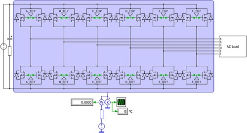
Figure 2. Six-phase T-NPC traction inverter topology.
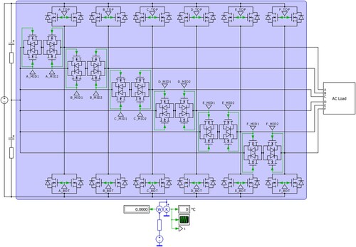
Both topologies are assembled from discrete semiconductor devices and due to the high current handling requirements, their parallel connection was necessary. One switching device is designed from two transistors with voltage blocking capability of 1200 Vdc. Voltage Source Inverter topology contains two switching devices per phase in a half-bridge connection. The T-NPC topology of the inverter is composed of four switching devices per phase, which are also parallelly connected. The two directly connected switching devices to the DC-Link must have the same power parameters as the half-bridge devices in the VSI topology. One bipolar switch has the blocking voltage capability reduced to half of the DC-Link voltage, what means that MOSFETs with 650 V blocking voltage will be enough. That’s because the switching devices connected directly to the DC-Link (TOP and BOT MOSFETs in both topologies) should be capable of withstand the blocking voltage level at the level of the DC-Link voltage, in this case 800 Vdc, while the switching devices connecting the output and neutral point of the DC-Link (MID MOSFETs in T-NPC), operating as a bidirectional switch, should be capable to withstand half the DC-Link voltage. Considering simulation analyses, symmetrical R-L load is being used.
2.2. Control system and working principle
Space vector pulse width modulation (SVPWM) is currently the primary control technique used in automotive traction drives. The derivation of this modulation can be found in [Citation5], and its usage in [Citation6]. For the two-level VSI topology, which is used today across the automotive industry, the SVPWM is easy to use since it contains 8 (2N, where N is the number of phases, in that case, 3) vectors. For three-level topologies (NPC and T-NPC) the number of vectors is 27 (3N, where N is the number of phases). However, with multi-phase multi-level topologies, the number of these vectors is high, what means that the difficulty of application of this modulation technique is increased compared to the standard three-phase two-level version. For a six-phase T-NPC topology, this would be 729 vectors that must be processed. Based on these facts it was decided that Sinusoidal pulse width modulation will be used instead of space vector PWM.
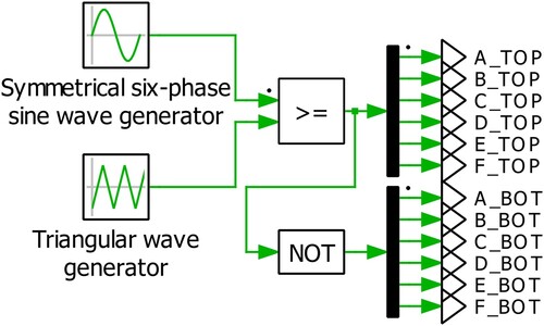
A control system block diagram for two-level VSI topology is shown in Figure . The symmetrical six-phase sine waves with an amplitude of 0.83 and 60 ° phase shift (in both control systems) is compared with the triangular carrier, which creates a six-phase two-level sinusoidal PWM.
Figure 3. Sinusoidal PWM control system for six-phase VSI inverter.
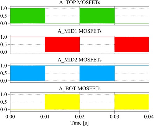
The triangular carrier in the two-level control system for VSI topology has an amplitude of 1. A block diagram of the whole control system for three-level inverter topology can be seen in Figure . The symmetrical six-phase sine waves in the three-level control system are compared with both positive (1–0) and negative (0 to −1) triangular carriers which make the six-phase three-level sinusoidal PWM. The six-phase output of the comparison of sinus waves and triangular carrier is subsequently divided through a demultiplexer into PWM for the individual phases of the inverter. For the three-level topology, the PWM signals for the individual phases must then be filtered by comparison with constant 0. An algorithm of this filtering is shown in the lower right part of Figure . The two-level PWM control signals for the individual switching devices of the A-leg of the VSI traction inverter topology are shown in Figure , and three-level control signals that drive A-leg of the T-NPC topology can be seen in Figure . These signals are the input signals for the gate drivers. To be able to see the switching pattern of the VSI topology driving signals, the time base of the Figure is 100 times lower than the time base of the driving signals of T-NPC thus providing detailed view on the gate driving pulses. This switching technique ensures the sinusoidal waveforms of the voltage and current variables within the load of the inverter. The closer look at switching process of the MOSFETs is shown in [Citation9], and [Citation14] with detailed MOSFETs parameters in [Citation13].
Figure 4. Sinusoidal PWM control system for six-phase T-NPC inverter.
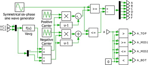
Figure 5. Sinusoidal PWM driving signals for A-leg of VSI traction inverter.
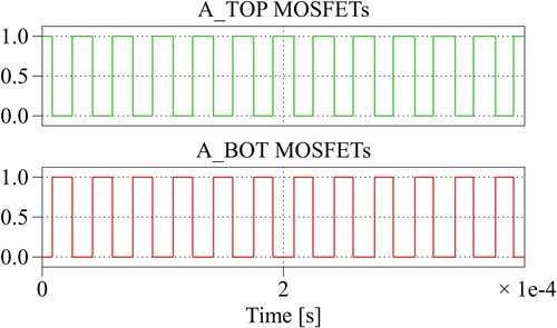
Figure 6. Sinusoidal PWM driving signals for A-leg of T-NPC traction inverter.
2.3. Thermal modelling of power semiconductor devices
To be able to perform simulation analysis of the power inverter losses in the simulation tool PLECS, it is necessary to create a thermal pad that covers the analyzed circuits’ semiconductor switching devices. This thermal pad is shown in Figure , or Figure and it is the blue platform, which is connected to the thermal components such as thermal resistor, thermometer, and source of constant temperature. These thermal parameters such as thermal resistance or constant ambient temperature were selected based on the real parameters of the heatsink commercially available and laboratory conditions. It is also very important for each semiconductor device to have a created or assigned thermal model with the value of the RDS(ON). The thermal model should contain information about the switching (turn-on and turn-off) and conduction losses of the semiconductor device. This information can be obtained from the component’s datasheet or additionally requested from the technical support of the given manufacturers. Some of the manufacturers have started offering these thermal models of their semiconductor portfolio freely available either from their website or from the website of the creator of PLECS.
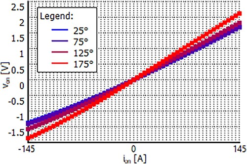
The graphical interpretation of the switching loss energy and conduction loss energy represented in Figures form the main part of the thermal model of Onsemi’s NTBG015N065SC1 semiconductor switching devices that operate in the analyzed circuit as bidirectional switches (MID1 and MID2) in T-NPC topology. In the same way, a thermal model for the used semiconductor switching device NTBG020N120SC1 also from Onsemi was designed. The second mentioned device is used in both power inverter topologies, directly connected to the DC-Link. Individual characteristics have been designed according to the datasheet information provided by the transistor manufacturer.
Figure 7. Turn-on loss energy of NTBG015N065SC1 in PLECS thermal domain.
Figure 8. Turn-off loss energy of NTBG015N065SC1 in PLECS thermal domain.
Figure 9. Forward characteristic of NTBG015N065SC1 in PLECS thermal domain.
The thermal models are not only important for power loss calculations, but also can help with the design of the thermal management for the inverter since the thermal management is very important in automotive. Both simulation models were designed thanks the thermal domain, more specific the junction temperature of MOSFETs and temperature of the simulated heatsink. Based on these temperature values both inverters were designed to be able to reliably work using the cooling system imported to the simulation models.
2.4. Efficiency evaluation settings
Since version 4.7, PLECS has provided a single block, called Switch Loss Calculator, which can calculate power losses of semiconductor devices. Depending on the user’s preference, the block can produce the output of conduction losses, switching losses (which can be further categorized into turn-on and turn-off losses), or total losses. A previous method for power loss analysis of the circuit in PLECS, used before version 4.7, is described in [Citation11]. Given that the results of both methods were identical, it is assumed that a system as mentioned in [Citation11] was used when creating a separate block for calculating the power losses of semiconductor components. The method used in the given literature compared the simulation results with the results expressed by manual calculation of switching and conduction losses, while the accuracy was reached at the level of 99%, which can be considered an accurate calculation by PLECS.
Figure shows the Switch Loss Calculator block, including its settings and display. The block only requires one parameter to be set, which is the average sampling period for the losses. Multiple semiconductor devices can be inserted into this block, and the output will be the sum of their selected power losses, which makes the calculation of the total power losses of the inverter easier (Figure ).
Figure 10. Power losses calculation block with its settings.
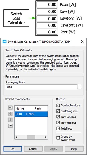
Adding components for calculating power losses in PLECS is the same as adding components to probes. Simply dragging a given semiconductor component to the probed components list will add the given component to the power loss calculation block. In this way, all used semiconductor switching devices were added to this block, from the output of which the total power losses of both proposed topologies were obtained.
3. Verification of the operational principle of the inverter topologies
The input parameters that were chosen for the power performance analysis of both circuits are shown in Table . These parameters are based on the future trends in the automotive traction inverter for a personal vehicle. The output power changes were carried out by changing the AC load while the power factor was conserved.
Table 1. Input parameters.
To demonstrate the designed simulation models of the inverter systems functionality, output parameters on the AC resistive-inductive load have been observed. Voltages and phase currents on the AC load were obtained at 50 kW continuous output power for both topologies. Figure shows the line to neutral voltages of the VSI inverter. Each of the phase voltage is recorded. Figure shows the line – to – line voltage. In order to identify differences between VSI and T-NPC inverter, similar interpretation of the time waveforms of the voltages are shown on Figures and for T-NPC inverter.
Figure 11. VSI traction inverter line-to-neutral voltages at 50 kW output power.
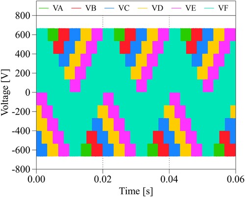
Figure 12. VSI traction inverter line-to-line voltages at 50 kW output power.
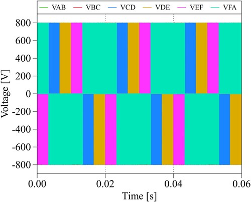
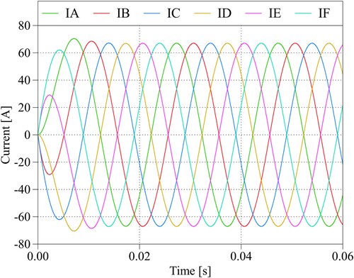
Since the output current waveforms of both topologies are identical because of the symmetrical AC load (Figures and ), the main difference between the two analyzed topologies output parameters is only visible at the line-to-neutral voltages. VSI topology line-to-neutral voltages (Figure ) consists of six levels (0, 1/6VDC, 1/3VDC, 1/2VDC, 2/3VDC, and 5/6VDC), which is due to number of phases, while the T-NPC (Figure ) line-to-neutral voltages is two-level (0 and 1/2VDC). The line-to-line voltage of VSI topology is characterized by two levels, i.e. nominal VDC and 0 VDC (Figure ). On the other side, Figure shows that the line-to-line voltage of T-NPC converter has 3 levels waveform, i.e. 0, 1/2VDC, and VDC.
Figure 13. VSI traction inverter phase currents at 50 kW output power.
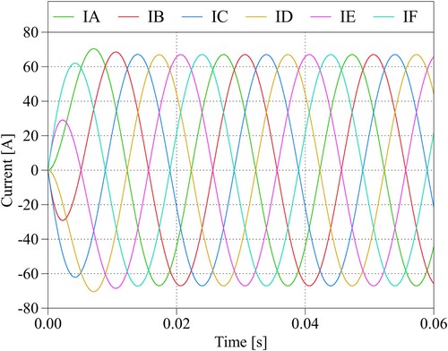
Figure 14. T-NPC traction inverter line-to-neutral voltages at 50 kW output power.
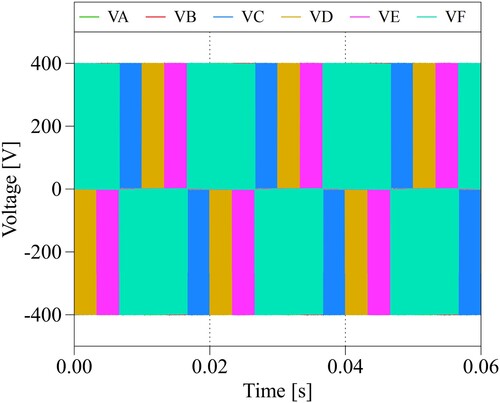
Figure 15. T-NPC traction inverter line-to-line voltages at 50 kW output power.
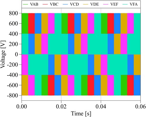
Figure 16. T-NPC traction inverter output currents at 50 kW output power.
Simulation results of the time-waveforms of the line-to-line voltages for both topologies are corresponding to the [Citation17], where the three-phase laboratory prototypes of two-level and three-level inverter topologies were experimentally verified and compared.
Based on the simulation results, the selection of components for the eventual physical implementation of the circuit is simplified. In addition to the waveforms of electrical quantities, it is possible to directly calculate their RMS values, providing another key parameter necessary for the proper selection of components for use in the given circuit. Apart from these output parameters, the calculation of the other important parameters can be performed. The calculation of the power factor, phase shift, or apparent or idle power is valuable for the system verification under various operational conditions. Part of the performance analysis of the circuit is also the analysis of the electrical parameters of the individual components within the main circuit. The voltage waveforms of each A-leg MOSFET of both topologies can be seen in Figures and . Because the drain to source voltage of the power transistor for VSI inverter has two levels, the shorter operational interval (100 times lower than T-NPC A-leg MOSFETs voltages) is provided here, while drain to source voltage waveform for T-NPC has longer time interval in order to identify individual voltage levels. According to these waveforms and the subsequently calculated effective values of these electrical parameters of the circuit semiconductor switching devices, it is possible to easily choose the necessary circuit components for practical implementation. The selection should be based on the maximum mentioned effective values (at maximal output power of the systems) to prevent any damage, that could happen with a bad choice of components. The determined range of the effective values at the continuous output power range for both topologies are indicated in Table . Voltage-blocking sustainability of the individual transistors is the key selection parameter. Achieved results reflect the operational principle of the converters. As shown in Table with VSI topologies, the RMS voltage is higher on the switching devices connected directly to the DC-Link. In T-NPC topology, the RMS values of the voltages of solid-state switching devices connected directly to the DC-Link are slightly lower when using the same devices compared to VSI. Bipolar switch semiconductor devices have these values more than twice as low.
Figure 17. Voltages on the VSI inverter A-leg MOSFETs at all power levels.
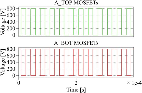
Figure 18. Voltages on the T-NPC inverter A-leg MOSFETs at all power levels.
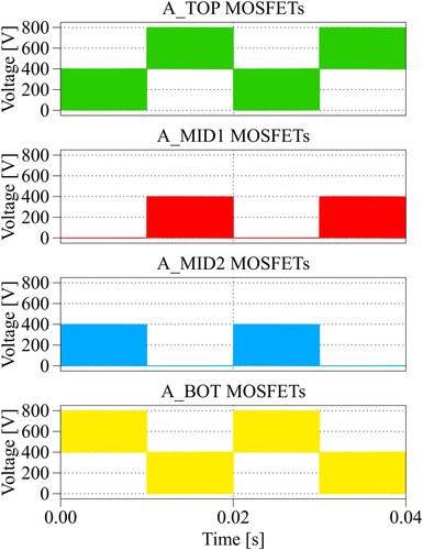
Table 2. Range of the effective values of A-leg MOSFETs voltages in both traction inverter topologies.
The RMS values of the voltages decrease slightly with increasing power, but due to this small decrease, these values could be considered constant for wide range of analyzed power levels. This also applies to the character and the values of the displayed voltage waveforms on individual transistors. These parameters of A-Legs are valid also for all other legs of the six-phase analyzed topologies.
The effective values of the transistor currents for both topologies are listed in Table . The effective current values of individual MOSFETs for the entire power range are higher with VSI topologies, which means that the criterion for selecting a MOSFET based on the value of the maximum current flowing through it will be higher. Comparable current load with MOSFETs of VSI topology is found on bipolar switch semiconductors. Here it can be observed that although their blocking voltage compared to MOSFETs directly connected to the DC-Link is lower, the current requirements have increased. The current waveforms, of which the RMS values were calculated, of both analyzed topologies A-Leg MOSFETs are displayed in Figures and . These waveforms are obtained at the 100 kW output power of both topologies. The current waveforms are obtained from only one of two parallel connected MOSFETs as one switch since the waveforms of both parallel connected MOSFETs are the same, but Table contains the total effective current in that one switch modelled with two MOSFETs.
Figure 19. Currents of the VSI inverter A-leg MOSFETs at 100 kW output power.
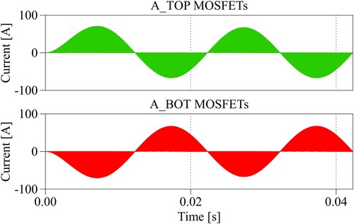
Figure 20. Currents of the T-NPC inverter A-leg MOSFETs at 100 kW output power.
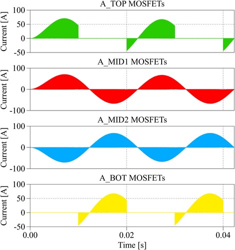
Table 3. Range of the effective values of A-leg MOSFETs currents in both traction inverter topologies.
4. Evaluation of the efficiency performance
The main part of the power performance analysis of the VSI and T-NPC topologies of the traction inverter is devoted to the power losses. These losses can be calculated after the assignment of thermal models and RDS(ON) values to each semiconductor switching device and placing them on the thermal pad in PLECS. Subsequently, thanks to the Switch Loss Calculator block, the power losses of the probed semiconductor devices are calculated. The circuits were analyzed at several power levels, while emphasis was placed on conduction, turn-on, and turn-off switching losses, the sum of which forms the total power losses. The total power losses of the whole VSI traction inverter can be seen in Figure . The same parameters of the T-NPC traction inverter are shown in Figure . All the necessary output data about power losses calculated in PLECS were extracted through the scope block to the comma separated values files and processed by a simple script in MATLAB environment.
Figure 21. Total power losses analysis of the VSI traction inverter.
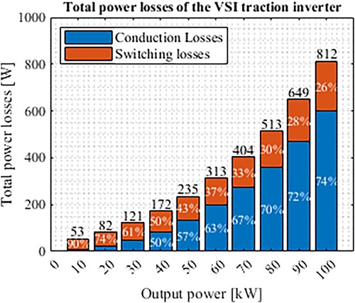
Figure 22. Total power losses analysis of the T-NPC traction inverter.
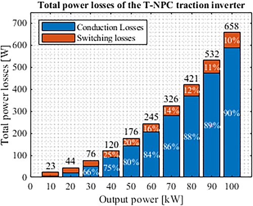
The total power losses of the Voltage Source Inverter topology below 40 kW output power mostly consist of switching losses. Above this value of the output power, the conduction losses are the majority. The maximal total power loss value is reached at the maximal output power, where the proportional part of the switching losses is the lowest. This is due to the larger step growth of conduction losses, which are dependent on the used material of the semiconductor devices.
As can be seen by the comparison of the total power loss figures, the T-NPC topology’s proportion of switching losses is lower compared to the VSI topology. While the switching losses in the VSI topology at output power above 40 kW begin to form a minority of the total power losses, in the T-NPC topology the switching losses form a minority already at values above 20 kW. Apart from the proportional side of the total power losses of both topologies, the comparison of their values makes the difference. The T-NPC topology reaches lower total power losses than the VSI.
The switching losses close-up detailed look of both main circuit’s topologies at divided losses to turn-on and turn-off for VSI topology is shown in Figure and for the T-NPC one in Figure , where the percentage ratio of their representation is expressed.
Figure 23. Switching power losses analysis of the VSI traction inverter.
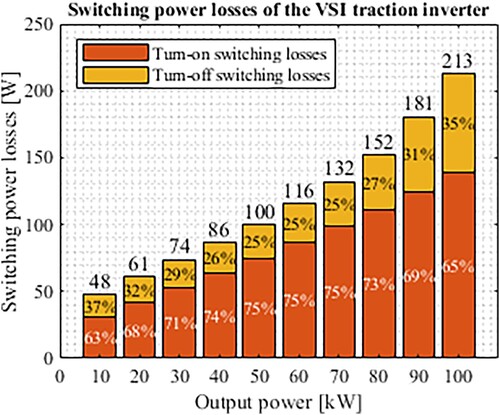
Figure 24. Switching power losses analysis of the T-NPC traction inverter.
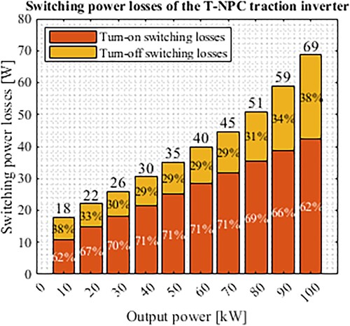
The proportion of turn-on and turn-off switching losses in both scenarios is close to the same, but as it was mentioned the total value of the switching losses in VSI topology at the same switching frequency is almost three times higher at all power levels.
Since power losses are calculated for each semiconductor device separately, it is also possible to graphically express, for example, the total losses of semiconductor devices of one leg of the main circuit of the inverter (can be seen in Figures and ).
Figure 25. VSI inverters A-leg total power losses.
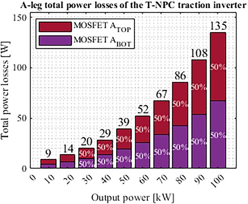
Figure 26. T-NPC inverters A-leg total power losses.
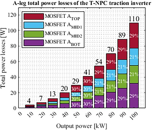
Total power losses of the one phase (A phase) for the VSI inverter show (Figure ) that the proportional division of the total power losses in these legs is equally divided between both switches. As this part of the analysis of A-Leg total power losses for the T-NPC inverter shows, even at lower power levels, the rise of the power losses at different power levels of each semiconductor device in one leg of the T-NPC topology is the same, which means that the proportional division stays the same at all output power values. The bigger part of the power losses in the analyzed leg are made by the semiconductor devices connected directly to the DC-Link.
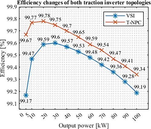
The main reason why these simulation models were designed and analyzed in the simulation tool PLECS is the efficiency evaluation. So, at the end of the power performance analysis, the efficiency of both traction inverter systems at increasing output power levels was shown graphically. This graphical representation of the efficiency changes depending on the output power is shown in Figure . As it can be seen, the efficiency values of the system are relatively high (more than 99%), considering the distributed amount of power. Both analyzed topologies are reaching high-efficiency values, but the T-NPC topology reached the maximal value at 20 kW output power. From the output of the analysis of power parameters of both traction inverter topologies, it is clear, that the three-level T-NPC topology achieves with the same input parameters as the VSI topology higher efficiency values at all output power levels. This parameter makes this topology an attractive alternative for automotive applications. But, compared with VSI topology it contains double the number of switching devices, which raises the total cost of its practical implementation. For the efficiency evaluation, the values for the 5 kW output power were added to a cleaner and clearer demonstration of the efficiency change behaviour of both inverters for output power change.
Figure 27. Efficiency evaluation of both analyzed traction inverter topologies.
5. Conclusion
In this paper, the commonly used across automotive traction drives traction inverter topology called Voltage Source Inverter, but enhanced to multi-phase, and multi-level converter in T-NPC topology were the main research issue. The main focus was given on the evaluation of the efficiency performance. As was mentioned, the target application is concentrated to e-mobility application. Design and development of power semiconductor systems is time and cost consuming within this area. In this paper a possible way how to evaluate the power semiconductor system performance is given. Discussed approach is based on the simulation modelling in time domain, while specific simulation tool was used. The selection of simulation software was undertaken according to requirements on the possibilities of fast and reliable computation. Because the main aim is determination of the efficiency performance of two analyzed power semiconductor converter topologies, a precise power loss model of power semiconductor devices is a must. The simulation tool has the thermal model library, which enables to define power losses of semiconductor devices within wide dependency on various circuit parameters (voltage, current, temperature etc …). Once the simulation models of power circuit is done, the evaluation of individual part of power transistors losses are evaluated for both topologies. The final result of this study is related to evaluation of the efficiency of VSI and T-NPC inverter. It is seen from the results, that T-NPC converter exhibits higher efficiency within the whole power range that was evaluated. It is seen that approximately 0.2% up to 0.5% efficiency value is higher even the higher amount of switching devices is presented within the main circuit of the T-NPC converter. Another advantage of multilevel inverter is better quality of electrical variables, thus lowering the negative impact on the electrical machine operation.
The presented design approach enables to analyse the performance of various operational experiments, while it presents a fast and reliable solution for multi-phase, multi-level power converter topologies investigation. The laboratory prototype of the 6-phase T-NPC inverter (100 kW) is currently under development. Within the future works, it is planned to provide more detailed and comprehensive analysis of the efficiency estimation utilizing different approaches (mathematical calculations, simulations and laboratory experiments).
Disclosure statement
No potential conflict of interest was reported by the author(s).
Additional information
Funding
References
- McKerracher C, O’Donovan A, Soulopoulos N, et al. Electric vehicle outlook 2022 [Online] Available: https://about.bnef.com/electric-vehicle-outlook/.
- Reimers J, Dorn-Gomba L, Mak C, et al. Automotive traction inverters: current status and future trends. 2019, IEEE Transactions on Vehicular Technology. p. 1–1. DOI:10.1109/TVT.2019.2897899.
- Sládeček V, Kuchař M, Palacký P. LiFePo battery charger with controlled rectifier. 2017 18th international Scientific Conference on Electric Power Engineering (EPE), Kouty nad Desnou, Czech Republic, 2017, p. 1–4. DOI:10.1109/EPE.2017.7967351.
- Cermak R, Kindl V, Laksar J, et al. Nine-phase induction motor with harmonic injection and different winding topology. 2020 international Conference on Electrical Machines (ICEM), Gothenburg, Sweden, 2020, p. 2125-2131, DOI:10.1109/ICEM49940.2020.9270999.
- Cacciato M, Consoli A, Scarcella G, et al. A novel space-vector modulation technique for common node emissions reduction. 2007 international Aegean Conference on Electrical Machines and Power Electronics, Bodrum, Turkey, 2007, p. 199–204, DOI:10.1109/ACEMP.2007.4510501.
- Palacky P, Baresova K, Sobek M, et al. The control system of electrical energy accumulation. 2016 elektro, Strbske Pleso, Slovakia, 2016, p. 346–349, DOI:10.1109/ELEKTRO.2016.7512094.
- Tran CD, Palacky P, Kuchar M, et al. Current and speed sensor fault diagnosis method applied to induction motor drive. IEEE Access. 2021;9:38660–38672. DOI:10.1109/ACCESS.2021.3064016
- Musznicki P, Turzynski M, Chrzan PJ. Accurate modeling of quasi-resonant inverter fed IM drive. IECON 2013 - 39th Annual Conference of the IEEE Industrial Electronics Society, Vienna, Austria, 2013, p. 376–381, DOI:10.1109/IECON.2013.6699165.
- Turzynski M, Kulesza WJ. A simplified behavioral MOSFET model based on parameters extraction for circuit simulations. IEEE Trans Power Electr. April 2016;31(4):3096–3105. DOI:10.1109/TPEL.2015.2445375
- Cacciato M, Caricchi F, Giuhlii F, et al. A critical evaluation and design of bi-directional DC/DC converters for super-capacitors interfacing in fuel cell applications. Conference Record of the 2004 IEEE Industry Applications Conference, 2004. 39th IAS Annual Meeting, Seattle, WA, USA, 2004, p. 1127–1133 vol.2, DOI:10.1109/IAS.2004.1348554.
- Frivaldsky M, Spanik P, Resutik P, et al. Comparison of loss behavior of discrete type and power module SiC transistor in 3-phase NPC converter. 2022 international Symposium on Power Electronics, Electrical Drives, Automation and Motion (SPEEDAM), Sorrento, Italy, 2022, p. 517–522, DOI:10.1109/SPEEDAM53979.2022.9842121.
- Pulvirenti M, Salvo L, Sciacca AG, et al. Modeling of SiC-MOSFET converter leg including parasitics of printed circuit board layout and device packaging. 2020 22nd European Conference on Power Electronics and Applications (EPE'20 ECCE Europe), Lyon, France, 2020, p. P.1-P.10, DOI:10.23919/EPE20ECCEEurope43536.2020.9215618.
- Musznicki P, Rucinski M, Turzynski M, et al. Prediction of ringing frequencies in DC-DC boost converter. 2016 international Symposium on Electromagnetic Compatibility – EMC EUROPE, Wroclaw, Poland, 2016, p. 672–675, DOI:10.1109/EMCEurope.2016.7739254.
- Turzynski M, Haras M, Kostro G, et al. A wide-band modeling of DC-DC two-transistor flyback converter. 2011 IEEE International Symposium on Industrial Electronics, Gdansk, Poland, 2011, p. 113–118, DOI:10.1109/ISIE.2011.5984.
- Simcak J, Frivaldsky M, Resutik P. Design of piece-wised linearized simulation model of the traction inverter suited for efficiency performance evaluation. 2023 international Conference on Electrical Drives and Power Electronics (EDPE), The High Tatras, Slovakia, 2023, p. 1–6, DOI:10.1109/EDPE58625.2023.10273866.
- U.S. Department of Energy. Electrical and electronics technical team roadmap, October 2017 [Online] Available: https://www.energy.gov/sites/default/files/2017/11/f39/EETT%20Roadmap%2010-27-17.pdf.
- Chen L, Ge B. High power traction inverter design and comparison for electric vehicles. 2018 IEEE Transportation Electrification Conference and Expo (ITEC), Long Beach, CA, USA, 2018, p. 583–588, DOI:10.1109/ITEC.2018.8450259.