
Abstract
We report on electrospinning of As3S7 chalcogenide glass from propylamine solution. The prepared glass layers consist of nanofibers with a typical diameter of ~100 nm. The deposited layers are highly porous from the nature of the electrospinning process. The calculated effective-refractive index value of the layers is n ~1·165, at λ = 1550 nm; assuming 87 vol.% of the air and the bulk glass index n = 2·27 at the same wavelength. In contrast to the continuous 2-micron thick spin-coated layer, which had the absorption edge near 420 nm, the 10-micron thick porous nanofibrous layer had no significant absorption edge at all. The relative stiffness of electrospun glass nanofibers was found to be 98% of the value measured for the bulk glass of the same composition. So far, electrospinning is the only solution-based technique, which directly deposits solvent-free chalcogenide glass layers with no need for any post-deposition annealing.
Introduction
In recent two decades, researchers all over the world have been relooking at a century old process [Citation1–3], currently known as electrospinning, that is able to produce continuous fibre layers with nanometer to micrometer diameter. Nanofibers and nanowires, large surface to volume ratio, have the potential to significantly improve current technology, for example catalysis, tissue scaffolds [Citation4], protective clothing, filtration and nano-electronics [Citation5], etc. Electrospinning is able to fabricate various nanofibers assemblies in situ, which allows for customization of nanofiber assemblies to meet the requirement of specific applications. Other methods of fabricating nanofibers, such as phase separation [Citation6] and template synthesis [Citation7], cannot match electrospinning in terms of its versatility, flexibility and ease of nanofibers production. Of the major classes of materials, electrospinning is able to produce nanofibers of polymers, composites, semiconductors and ceramics [Citation8, 9]. A good summary of papers on electrospinning, and nanofibers fabrication can be found in the book by Ramakrishna et al. [5] (and references therein). The fundamentals of electrospinning process, influence of spinning conditions on the resulting morphology, and characterization of nanofibers for various applications can be found in Refs. [Citation10–12]. Recent research effort in electrospun fibers has been focused on exploring new materials which can be spun, characterization of the fibers and identifying new applications of the fibrous materials. It is important to fabricate various fibrous assemblies, because the fiber arrangement has significant effect on the performance of new devices. The development of the ordered (aligned) nano-grooves and assemblies has been shown to influence cell proliferation and morphology [Citation13], and found application in the form of aligned fibers in muscle regeneration [Citation14].
Most produced electrospun nanofibers are based on polymers or inorganic materials such as crystalline semiconductors [Citation8, 9]. There are a few examples of electrodeposition of glasses [Citation15–17]. Electrospinning of silica glass nanofibers was done by using a technique resembling sol–gel process with a calcination step after the deposition [Citation15]. Low melting point borate glasses were prepared in the form of nanofibers by melt-spinning process at temperature of 850 °C [Citation16]; such high temperatures are necessary in order to have low viscosity melt suitable for electrospinning. Glass nanofiber materials can also be prepared by pyrolysis of polymeric nanofibers such as SU8 resist, for example as it was demonstrated by J. E. Clark for glass-carbon nanofibers [Citation17].
Preparation of polycrystalline semiconducting chalcogenides nanofibers, among the existing chalcogenide materials, has been reported: (i) by electrospinning of a polymer followed by a galvanic displacement of Bi2Te3 [Citation18] used for thermo-electric applications, (ii) by electrospinning from solution mixtures with polymers, and (iii) by electrospinning of semiconducting chalcogenides such as Bi2S3, ZnS [Citation19] for applications in novel sensors, super-capacitors, or batteries.
In this paper, we describe preparation of isolated nanofibers and/or nanofibrous layers of amorphous chalcogenide [Citation20] As3S7 by electrospinning from propylamine solutions of the glass. The layers were deposited directly without a need for employing other processed such as sintering or pyrolysis of precurssors or galvanic displacement of polymer nanofiber templates for inorganic material as it is usual in the case of fabrication of nanofibrous layers of semiconducting chalcogenide materials [Citation18, 19].
Experimental
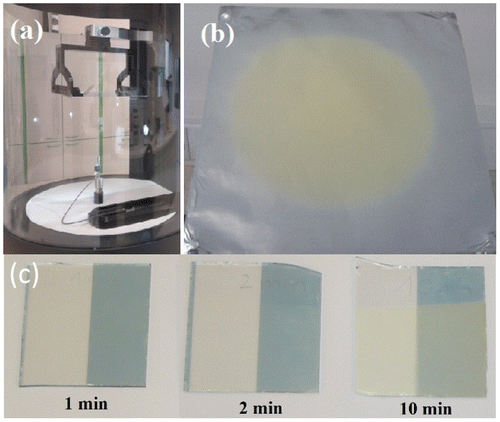
Chalcogenide glass, mass of 1 g, of the composition As3S7 was spontaneously dissolved in 2 mL of propylamine at room temperature for 24 h. The formed solution has dark brown color and honey-like viscosity. Films were deposited by an electrostatic spinning apparatus 4SPIN® LAB1, Contipro a.s, Czech Republic. The formed solution was dispensed from a syringe with volume of 10 ml through the needle of 26 Gauge with a feeding rate ~5 μL min−1. The needle was connected to a high-voltage source with a set voltage in the range of 25‒35 kV. Temperature and relative humidity in the deposition chamber was kept in the range of 22 ± 2 °C and 30 ± 5% RH, respectively. The chalcogenide glass nanofibrous layers were deposited onto a collector surface placed oppositely to the needle, as shown in Figure . The distance between the needle and the collector was 15–20 cm. A grounded metal plate 20 × 20 cm was used as the collector. A rotating collector, accelerated at speeds up to 4000 rpm, was used for the deposition of aligned nanofibers. Aluminum foils attached to the metal plate and the rotating collector were used as substrates. Microscope glass slides coated with conductive ITO/FTO films were used as substrates for deposition of samples intended for optical transmission measurements. Deposition times were 1, 2, 5, 10 and 20 min resulting in formation of either isolated nanofibers or nanofiber layers on the substrates. One half of the samples was then coated with 3 nm thick Au layer by thermal evaporation.
Figure 1. (a) Photo of the As-S glass electrospinning experimental setup (b) Photography shows a As-S glass nanofiber layer electrospun for 10 min on Al foil substrate with the diameter of the layer ~15 cm. (c) Images show layers spun for 1, 2 and 10 min. The right-hand side of the samples were coated with a 3 nm thin Au layer after the electrospinning (Color online).
Scanning electron microscope (SEM) images revealing morphology of the glass nanofibers or nanofiber layers were recorded by using an Ultra Plus (Zeiss, Germany), equipped with a field-emission gun, at a low accelerating voltage of ~1 kV. Atomic-force microscope (AFM) was done on isolated glass nanofibers by employing a Solver Pro M (NT-MDT, Russia) device. The measurements of surface topography, atomic-force acoustic microscopy (AFAM) and force spectroscopy (FS) measurements were carried out using a high-resolution silicon cantilevers type CSG-10 (Au coating, a cone angle less than 22°; a typical force constant of 0·1 N m−1) in the contact mode. The optical transmission spectra were recorded on a UV/Vis/NIR spectrophotometer Jasco 570 in the range of wavelengths from 200 to 1800 nm.
Results and discussion
Macroscopically, all prepared nanofibrous samples look as continuous yellowish layers (Figure ). Nanofibrous morphology of the electrospun chalcogenide glass layers was confirmed by using the SEM as shown in Figure . Figure , parts (a) and (b) shows isolated nanofibers of As3S7 glass deposited on Al foil. The deposition time for these samples was 1 min. Figure , parts (c)–(f) shows unaligned nanofibers, parts (c) and (e) – the metallic plate collector substrate, and aligned nanofibers, parts (d) and (f) – the rotating collector substrate, orientations of the glass nanofibers in 10 μm thick layers spun for 20 min. The electrospinning process ran smoothly, resembling the deposition process of polymer nanofibrous layers from solutions. The solution of As3S7 glass could be spun without applying any of the supporting procedures, e.g. co-spinning with easy spinable material, air blowing, and external drying, which are used to help unspinable solutions to form nanofibers. Since the glass solution viscosity and low molecular weight of the glass structural units, the yield of the electrospinning process is rather low (at low spinning rates of ~5 μL min−1) in comparison to the spinning efficiencies which can be achieved for well-spinable polymers such as PVA and PEO.
Figure 2. SEM micrographs of the chalcogenide As-S glass isolated nanofibers and nanofiber layers prepared by electrospinning of the glass solution on Al foil substrate. The spinning times were (a) and (b) 1 min, (c)–(f) 20 min for stationary, parts (a)–(c), (e), and rotating, parts (d) and (f) collectors.
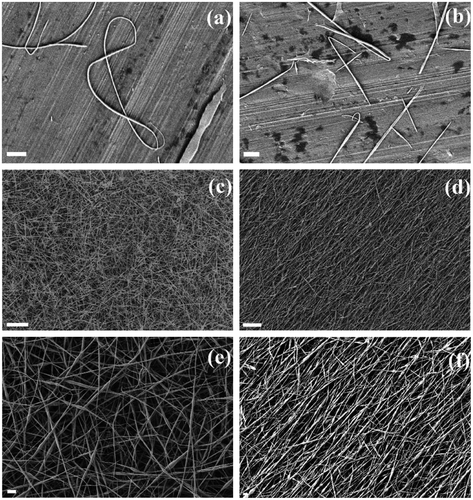
Figure (a) shows comparison of optical transmittance spectra of the chalcogenide As3S7 glass nanofibrous layers after 1, 2 and 10 min of deposition, a 2 μm thick spin-coated layer of As3S7 glass, a 100 nm thick spin-coated layer of As3S7 glass (both spin-coated layers were deposited onto microscope slides; annealed at 120 °C for 10 h; details of the spin-coating deposition and the densification process of the layers can be found in Ref. [Citation21]) and the As3S7 bulk glass. In the high absorbing region of the glass, i.e. 400–470 nm, the continuous spin-coated layer has the absorption edge near 420 nm, while the porous nanofibrous layer has no significant absorption edge at all. This is because the nanofibrous layer is highly porous and its effective-refractive index is the combination of the indices of the air and the glass. The effective-refractive index of the nanofibrous layer spun for 20 min (referred in the text also as 10 μm thick layer) of As3S7 glass was calculated to be n ~1·165 assuming 87 vol.% of the air in the pores of the layer and the bulk glass n = 2·27, all at λ ≈ 1550 nm. In comparison, the absorption edge of the well-annealed 100 nm thick spin-coated continuous layer is near λ ≈ 270 nm.
Figure 3. (a) Optical transmittance spectra of chalcogenide As3S7 glass aligned or unaligned nanofibrous layers after 1, 2 and 10-min deposition onto the silica glass slides substrates coated with ITO/FTO are shown in comparison with of 100 nm and 2 μm spin-coated layer onto a microscope slide, and the bulk glass. (b) Optical transmittance spectra of the chalcogenide As3S7 glass nanofibrous layers after 1, 2 5 and 10 min of deposition are shown in comparison with the same layers coated with a 3 nm layer of gold and a 3 nm single-layer of gold f.
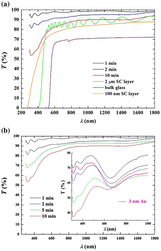
Figure (b) shows the optical transmittance of nanofibrous layers of As3S7 glass after 1, 2, 5 and 10 min deposition in comparison with the spectra of the same layers (in the inset) coated with a 3 nm thin layer of gold and the spectrum of a 3 nm single-layer of gold. The characteristic surface plasmon resonance (SPR) of Au is apparent near λSPR = 674 nm for the metallic layer with a slight blueshift when the gold was deposited on top of the glass nanofibrous layers, i.e. ΔλSPR ~23 and 11 nm for the layers deposited for 1 and 2 min, respectively. The layer deposited for 5 min has nearly negligible shift of ΔλSPR ~4 nm; the layer deposited for 10 min shows the blue shift of ΔλSPR ~37 nm. The SPR band intensity decreases with increasing thickness of the deposited As3S7 glass nanofibrous layers.
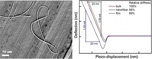
The atomic-force microscopy measurements performed on the isolated As3S7 nanofibers reveal the typical diameter of the nanofibers to be in the range of 100‒130 nm; the length was estimated in the range of 1‒15 μm (Figure ). Figure (a) and (b) show topography of the isolated As3S7 nanofibers, i.e. for 1 min deposition, scans taken from 7·5 × 7·5 μm2 and 2·5 × 2·5 μm2 areas, respectively. Figure (c) shows a profile, extracted from Figure (a), of a representative nanofiber with the height of the probed nanofiber to be ~115 nm and its width ~110 nm. AFM technique is capable of recording information from the sample surfaces in various modes including the acoustic-AFM (AFAM) AFAM signal corresponds to the shift of the flexural resonance of the tip-sample system due to the changes of the surface and near sub-surface local elastic moduli of the material responding to the forced out-of-plane vibration emitted by an external ultrasound transducer [Citation22]. The tip is repulsed in the linear part of the force-distance curve, which is related to the Hooke’s law (F = −k × Δ), and the slope corresponds to the stiffness of the material. The relative stiffness of the As3S7 bulk glass, a spin-coated As3S7 thin film annealed at 120 °C for 10 h and the electrospun As3S7 nanofiber (time?) was estimated from the slope of the lines in the plot of the dependence between the deflection of the tip versus the measured piezo-crystal displacement. The curves, plotted in Figure (d), represent the averaged values recorded from five consecutive measurements on five different places of the samples; parts of the nanofibers firmly attached to the substrate were measured.
Figure 4. (a) and (b) AFM topography of chalcogenide As3S7 glass nanofibers deposited for 2 min. (c) The profile recorded from the nanofiber shown in part (b). (d) The dependence of the tip deflection on the piezo-displacement; the region of the repulsive interactions is used to compare the relative stiffness of the As3S7 bulk glass, the well-annealed spin-coated film and the electrospun chalcogenide nanofiber (Color online).
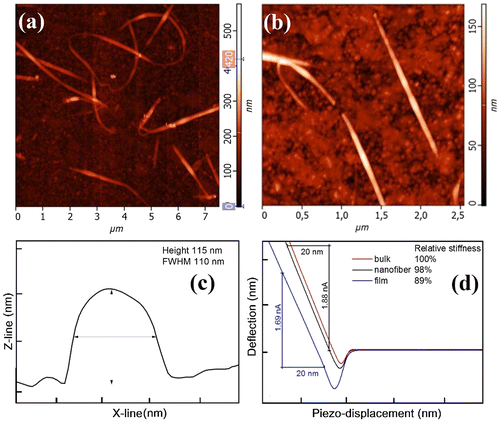
The stiffness of the As3S7 nanofibers is ~98% of the stiffness values obtained for the bulk glass. The relative stiffness of the well-annealed spin-coated film, still containing noticeable amount of the solvent, was determined to be ~89% of the value determined for the bulk glass. The glass nanofibers have stiffness of the bulk glass, despite the fact that the nanofibers did not undergo any post-deposition annealing procedure. This is the indirect evidence for obtaining the solvent-free chalcogenide glass layers by electrospinning process. So far, solvent-free layers of chalcogenide glasses have not been achieved by any of the other solution deposition techniques [Citation23, 24].
The common limitation for the use of solution-processed chalcogenide glasses in the real applications, for example as waveguides, ring resonators and in nonlinear optical devices, stems from the inefficient release of a solvent, typically butylamine and propylamine, from the glass network even after pro-long annealing at temperatures close to the glass-transition temperature [Citation23]. This is the issue especially for spin-coated and ink-printed thin-film chalcogenide glass optical components reported elsewhere in the literature [Citation23, 24], where the effects of chalcogenide/solvent pair choice and influence of the annealing conditions on thin film properties are properly discussed.
In our opinion, electrospinning may become a new route of room temperature and annealing-free solution processing of chalcogenide glass layers. Potential application of electrospun chalcogenide nanofibers can be proposed, e.g. in (i) chemical sensing – by exploiting the high porosity and high surface area of sulfur-based nanofibers (ii) batteries, where sulfur-based compounds are proposed as the promising cathode materials for high-capacitance batteries in combination with high-performance solid-state electrolytes (iii) optics by exploring the optical and optomechanical properties of chalcogenide glass nanofiber layers and aligned nanofibers.
Conclusions
We have clearly demonstrated that solvent-free nanofibrous layers of chalcogenide As3S7 glass can be electrospun from propylamine solutions at room-temperature, in the air atmosphere and without a need for post-deposition annealing. Electrospinning of the glass nanofibers from amine solutions is possible mainly due to the ability of As3S7 glass to form a viscous solution in propylamine, high volatility of the solvent, strong effect of the electro-static field on the solvent removal from the nanofibers and finally the polymer-like structure of the glass. The electron and atomic-force microscopies revealed the typical diameter of the nanofibers around 100 nm and the lengths in micrometer order for the isolated nanofibers deposited for 2 min. The relative stiffness of As3S7 glass nanofibers was found to be ~98% of the value for the bulk glass, which promises a good material mechanical stability in potential applications.
Disclosure statement
No potential conflict of interest was reported by the authors.
References
- Doshi J, Reneker DH. Electrospinning process and applications of electrospun fibers. J Electrost. 1995;35:151–160.10.1016/0304-3886(95)00041-8
- Cooley JF; Apparatus for electrically dispersing fluids. US Patent Specification. 692631. 1902
- Morton WJ; Method of dispersing fluids. US Patent Specification. 705691. 1902.
- Wang YK, Yong T, Ramakrishna S. Nanofibers and their influence on cells for tissue regeneration. Aust J Chem. 2005;58:704–712.10.1071/CH05222
- TeoWE, and RamakrishnaS. A review on electrospinning design and nanofibre assemblies. Nanotechnology, 2006; 17: R89–R106.
- Witte D, Dijkstra PJ, Berg JW, et al. Phase separation process in polymer solutions in relation to membrane formation. J Membr Sci. 1996;117:1–31.10.1016/0376-7388(96)00088-9
- Chakarvarti SK, Vetter J. Template synthesis-membrane based technology for generation of nano-/micro materials: a review. Radiat Meas. 1998;29:149–159.10.1016/S1350-4487(98)00009-2
- Chronakis IS. Novel nanocomposites and nanoceramics based on polymer nanofibers using electrospinning process – A review. J Mater Process Technol. 2005;167:283–293.10.1016/j.jmatprotec.2005.06.053
- Larsen G, Velarde-Ortiz R, Minchow K, et al. A method for making inorganic and hybrid (organic/inorganic) fibers and vesicles with diameters in the submicrometer and micrometer range via sol−gel chemistry and electrically forced liquid jets. J Am Chem Soc. 2003;125:1154–1155.10.1021/ja028983i
- Hohman MM, Shin M, Rutledge G, et al. Electrospinning and electrically forced jets. I. Stability theory. Phys Fluids. 2001;13:2201–2220.10.1063/1.1383791
- Tan SH, Inai R, Kotaki M, et al. Systematic parameter study for ultra-fine fiber fabrication via electrospinning process. Polymer. 2005;46:6128–6134.10.1016/j.polymer.2005.05.068
- Desai K, Lee JS, Sung C. Nanocharacterization of electrospun nanofibers of polyaniline/poly methyl methacrylate blends using SEM, TEM and AFM. Microsc Microanal. 2004;10:556–557.10.1017/S1431927604881558
- Kongkhlang T, Tashiro K, Kotaki M, et al. Electrospinning as a new technique to control the crystal morphology and molecular orientation of polyoxymethylene nanofibers. J Amer Chem Soc. 2008;130:15460–15466.10.1021/ja804185s
- Aviss KJ, Gough JE, Downes S. Aligned electrospun polymer fibers for skeletal muscle regeneration. Eur Cells Mater. 2010;19:193–204.10.22203/eCM
- Wang M, Jing N, Su CB, et al. Electrospinning of silica nanochannels for single molecule detection. Appl Phys Lett. 2006;88:033106-1–033106-3.10.1063/1.2165277
- Praeger M, Saleh E, Vaughan A, et al. Fabrication of nanoscale glass fibers by electrospinning. Appl Phys Lett. 2012;100:063114-1–063114-3.10.1063/1.3684940
- Clark JE, Olesik SV. Electrospun glassy carbon ultra-thin layer chromatography devices. J Chromatogr A. 2010;1217(27):4655–4662.10.1016/j.chroma.2010.04.078
- Lee K-J, Song H, Lee Y-I, et al. Synthesis of ultra-long hollow chalcogenide nanofibers. Chem Commun. 2011;47:9107–9109.10.1039/c1cc12312b
- Entradas TJ, Cabrita JF, Barrocas B, et al. Synthesis of titanate nanofibers co-sensitized with ZnS and Bi2S3 nanocrystallites and their application on pollutants removal. Mater Res Bull. 2015;72:20–28.10.1016/j.materresbull.2015.07.008
- Adam J-L, Zhang X. Chalcogenide glasses: preparation, properties and applications. Oxford: Woodhead Publishing; 2014.
- Kohoutek T, Orava J, Strizik L, et al. Large-area inverse opal structures in a bulk chalcogenide glass by spin-coating and thin-film transfer. Opt Mater. 2013;36:390–395.10.1016/j.optmat.2013.09.026
- Zausher S, Parlak Z, Tu Q. Mapping the stiffness of nanomaterials and thin films by acoustic AFM techniques. In: Bhushan B, Luo D, Schricker SR, Sigmund W, Zauscher S, editors. Handbook of nanomaterials properties; 2014. p. 1023–1051. Berlin: Springer.
- Orava J, Kohoutek T, Wagner T. Deposition techniques for chalcogenide thin films. In: Adam JL, Zhang X, editors. Chalcogenide glasses: preparation, properties and applications; 2014. p. 265−309. New Delhi: Woodhead. 10.1533/9780857093561.1.265
- Sanchez EA, Waldmann M, Arnold CB. Chalcogenide glass microlenses by inkjet printing. Appl Opt. 2011;14: 1974–1978.