
ABSTRACT
Two-dimensional (2D) materials emerged in the last decade have been considered as an attractive class of gas sensing materials due to their large surface-to-volume ratio, high surface reaction activity and good gas adsorption performance provided by the atomically thickness and flat surface. The development of high-performance micro-nano gas sensors places higher demands on sensing materials, thus 2D materials must satisfy good sensing performance requirements such as excellent gas selectivity, reproducibility, long-term stability, and fast response/recovery time to achieve high sensitivity detection at low concentrations. Herein, we overview the recent literature on the sensor structure, sensing mechanisms and improved gas sensing performance of 2D materials-based gas sensors. In particular, we discuss how the sensing properties of 2D materials can be modulated through defect and doping engineering, modification with noble metal, constructing heterostructure, as well as external energy assistance, e.g. by light illumination. Besides reviewing the achievements of gas sensors based on 2D materials, we provide an outlook on their future developments. Understanding the relationship between structure and sensing mechanisms of 2D materials-based sensors provides vast opportunities for designing advanced gas sensors, making it promising for a wide range of practical applications.
1. Introduction
Owing to its ability to sensitively detect molecules at ultra-low concentrations, gas sensors have attracted huge interests of researchers and been widely used in many fields such as environmental monitoring, hazardous gas detection, industrial production, and medical diagnosis [Citation1–5]. The sensing material, as the core of the sensor, determines the performance of the device. Among various sensing materials, semiconducting metal oxides are most common in gas sensors due to their facile preparation and low manufacturing cost [Citation6–9]. However, gas sensors based on semiconducting metal oxides suffer high operating temperature (usually 200°C to 500°C), long recovery time and poor selectivity, which limit their practical application [Citation10,Citation11]. Therefore, it is highly desirable to develop novel gas sensors with high selectivity and fast response at room temperature.
Two-dimensional (2D) materials have tremendous advantages in gas sensing. Firstly, the inherent atomically thickness of 2D materials leads to ultra-high surface-to-volume ratio, which is beneficial for gas sensors to exhibit excellent performances such as high sensitivity, low detection limits, and fast response/recovery rates [Citation12–14]. Secondly, different from conventional semiconducting sensing materials that rely on chemical reactions with gas molecules to achieve gas sensing, most gas sensors based on 2D materials relies on direct charge transfer, making gas sensing workable at room temperature conditions [Citation15,Citation16]. Besides, 2D materials exhibit excellent compatibility in ultra-thin silicon channel technology and have been considered as promising candidates for the manufacturing and integration of gas sensor devices [Citation17,Citation18]. What’s more, the properties of 2D materials like morphology, structure, bandgap and carrier mobility can be easily modulated by defect engineering and doping [Citation19,Citation20], which provides new approaches to improving gas sensing performances and achieving more practical applications. For instance, p-type and n-type 2D materials exhibit different sensitivities to gases owing to the various band structures. n-type 2D semiconductors are sensitive to electron donors such as O2 and NH3, while p-type 2D semiconductors are sensitive to hole donors such as H2S and NO2, which is favorable for designing highly sensitive gas sensors [Citation21,Citation22].
In the last decades, 2D materials have been rapidly developed with the increasing variety, including classical graphene [Citation23], borophene [Citation4], transition metal dichalcogenides (TMDs) [Citation24], black phosphorus (BP) [Citation25], boron nitride (BN) [Citation26], and emerging MOFs [Citation27,Citation28] and MXenes [Citation29], providing a rich material selection for gas sensing manufacturing, which can be proved through the number of published papers. A comprehensive literature search was conducted in Web of Science since 2000, using the topic ‘2D materials for gas sensors’. As shown in , the number of articles has been rapidly increasing since 2010 and has continued to grow exponentially especially in recent years from approximately 11 articles published in 2010 to 300 articles in 2022, showing the great prospects of 2D materials in gas sensing field. Moreover, with the development of nanotechnology, methods for large-scale preparation of 2D materials are becoming more mature, allowing precise control of thickness and number of atomic layers, such as exfoliation method, chemical vapor deposition (CVD), physical vapor deposition (PVD), etc., accelerating the practical application of 2D material gas sensors [Citation30–32]. Although 2D materials have made great progress in gas sensing, there are still some limitations hindering their application. For example, the huge specific surface and ultra-high reactivity easily lead to the indifferent adsorption when exposing different gas atmosphere, resulting in poor selectivity [Citation33]. Besides, gas molecules are hard to desorption from the surface of 2D material without heating or illumination, leading to long recovery time at room temperature [Citation34]. As a result, the selectivity, room-temperature recovery rate, and the long-term stability of fabricated gas sensors based on 2D materials still need to be further improved.
Figure 1. Records of the number of publications on the topic of 2D materials for gas sensors. (internet search from web of Science on October 31, 2023).

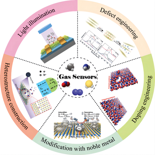
In this review, we first summarize the structure of gas sensors based on 2D materials. Secondly, the sensing mechanisms of gas sensors are detailed. Subsequently, the recent progress of strategies to improve the performance of 2D materials-based gas sensors is systematically introduced (), including defecting and doping engineering, modification with high work function noble metal, constructing heterostructure and external energy assistance. Lastly, the perspectives of 2D materials-based gas sensors are given in terms of the advantages and disadvantages of gas sensors. We believe that the comprehensive study of the sensing mechanisms and improvement measures for sensing performance of 2D materials-based gas sensing will provide new ideas for the development of 2D materials and be valuable to 2D material-based gas sensing fields.
Figure 2. Recent progress of strategies to improve performance of 2D materials-based gas sensors.

2. Sensor structure and testing method
Semiconductor gas sensors can be divided into two major categories based on their sensing mechanism: resistive and non-resistive sensors [Citation1,Citation35]. Concretely, as for resistive gas sensors, gas molecules interact with the device and change the resistance of the sensor to realize gas detection. Instead, non-resistive gas sensors utilize the physical and chemical reactions between the gas molecule and the sensing material to change other electrical parameters, such as the threshold voltage of a field effect transistor and the output characteristics of a diode, to detect the gas molecule. Among them, resistive gas sensors, with easy detection mechanism, have been extensively studied and applied in reported 2D materials [Citation36–38]. This section provides a brief depiction concerning resistive gas sensors with different structures and the related testing method.
2.1 Field-effect transistors (FETs)
The structural schematic of FET gas sensors based on 2D materials is illustrated in . The FET typically consists of a single 2D nanosheet deposited between the source and drain electrodes to form the sensing channel. The gate electrode is located on the other side of the substrate and is separated from the channel by a thin dielectric layer. Currently, the methods for preparing 2D sensitive materials are developing rapidly, including common methods such as mechanical exfoliation, chemical vapor deposition, atomic layer deposition, hydrothermal method, and solvent thermal method, which can successfully control the size and thickness of the materials as desired [Citation31,Citation40]. When a FET gas sensor interacts with gas molecules, the adsorption or reaction on the surface results in the movement of carriers, leading to alterations in electrical conductivity, volt-ampere characteristics, or surface potential. Through collecting and analyzing the change of resistance value, information such as gas composition and concentration can be obtained.
Figure 3. Schematic of the (a) FET and (b) heterojunction gas sensor based on 2D materials. (c) schematic diagram of the gas sensor test platform [Citation39].
![Figure 3. Schematic of the (a) FET and (b) heterojunction gas sensor based on 2D materials. (c) schematic diagram of the gas sensor test platform [Citation39].](/cms/asset/81c1cd06-56e2-42ca-a49c-a5024f6e2551/tapx_a_2288353_f0003_oc.jpg)
2.2 Heterojunction sensors
Heterojunction sensors are a novel class of gas sensors that consist of two different semiconducting sensing materials, and the structure is illustrated in . According to the conductivity type of semiconductors, heterojunctions can be classified into p-p type, p-n type, and n-n type. After two semiconductor materials contacting with each other, the Fermi level at the interface will balance to the same energy state. This process is accompanied by the transfer of charge carriers and the formation of a depletion or accumulation layer at the heterojunction. Different from traditional semiconductor materials, the surface of 2D materials has no dangling bonds, therefore, the formed heterojunction has a high-quality interface. Moreover, the carrier concentration and band alignment of 2D materials can be effectively modulated through electrical or optical means, providing new possibilities for expanding the application of heterojunction structures. A large number of studies have shown that constructing heterojunctions can effectively enhance gas sensing performance [Citation41,Citation42], which will be discussed in detail in the fourth section.
2.3 Testing method
In a typical gas sensing test process, the 2D material gas sensor is placed in a closed chamber and a certain test voltage is applied to the device to obtain the resistance value during the gas sensing. Then, the target gas is passed into the closed chamber. At this time, the resistance of the gas sensor will increase or decrease significantly due to the interaction between the 2D sensing material and the target gas. When the resistance value is stable, the target gas is discharged from the chamber, so that the entire chamber environment and the device resistance are restored to the initial state. During the whole process, a data acquisition system such as a computer is used to record the change of the resistance of the gas sensor in real time to obtain the corresponding sensing information, the corresponding test platform is shown in .
3. Sensing mechanism
3.1 Charge transfer
Charge transfer is the main mechanism of gas sensing in 2D materials. When the gas sensor is exposed to the target gas, charge transfer will occur between the sensing material and the gas molecule, as shown in [Citation43]. The direction of charge transfer and the amount of charge transferred are differentiated for different kinds of gases, resulting in distinct changes of the sensor to achieve gas identification and classification. In general, oxidizing gases (such as NO2, O2, Cl2, etc.) tend to take electrons from the surface of 2D materials [Citation45–47], while reducing gases (such as CO, H2, NH3, etc.) provide electrons to sensitive materials [Citation48–50]. When the sensor is exposed to the target atmosphere, the target gas molecules adsorb on the surface of the sensitive material with charge transfer, changing the resistance value of the sensor. On the contrary, when the target gas is removed, the target gas molecules already absorbed are desorbed from the surface of the material, so the resistance of the sensor is restored to the original state.
Figure 4. Schematic illustration of gas sensing mechanisms. (a) surface charge transfer model [Citation43]. (b) Schottky barrier modulation [Citation44]. (c) and (d) surface adsorption of oxygen ions
![Figure 4. Schematic illustration of gas sensing mechanisms. (a) surface charge transfer model [Citation43]. (b) Schottky barrier modulation [Citation44]. (c) and (d) surface adsorption of oxygen ions](/cms/asset/dac6bf31-949f-493f-b109-9decfe12cb0e/tapx_a_2288353_f0004_oc.jpg)
For p-type two-dimensional layered materials, when they are in contact with oxidizing gas molecules, the oxidizing gas tends to acquire electrons from the surface, resulting in an increase in the concentration of holes. As holes are the majority carrier for p-type semiconductor, an increase in conductivity can be observed. Conversely, when they are exposed to reducing gas molecules, their conductivity decreases. For n-type two-dimensional layered materials, the opposite change of conductivity in the device occurs. Typically, the surface charge transfer can be proven through computational simulations based on first-principles calculations using density functional theory (DFT) [Citation51,Citation52].
3.2 Schottky barrier modulation
Another mainstream explanation of the gas sensing mechanism of two-dimensional layered materials is the Schottky barrier modulation [Citation44,Citation53]. It means that the gas molecules adsorbed on the surface of two-dimensional materials will induce a built-in electric potential and modulate the Schottky barriers between 2D material and the electrode, as shown in . Taking n-type 2D materials as an example, when the surface electrons of the material are captured by the oxidizing gas such as NO2, the Fermi level of the n-type sensing material tends to move towards the valence band, which increase the Schottky barrier and reduce the built-in electric potential, resulting in a decrease in the electrical conductivity and an increase in the resistance of the sensing material. Conversely, when n-type 2D materials adsorb reducing gases (such as NH3) on their surface, electrons from gas molecules transfer to the material surface, causing the Fermi level of the material to move towards the conduction band, which reduce the Schottky barrier while increase the built-in electric potential, resulting in an increase in the electrical conductivity and a decrease in the resistance of the sensing material. As for p-type 2D materials where holes are majority carriers, the trend of the conductivity is opposite to that of n-type semiconductors.
3.3 Surface adsorption of oxygen ions
Surface adsorption of oxygen ions is also one of the gas sensing mechanisms for two-dimensional materials, commonly used in high-temperature or light-illuminated conditions for gas sensing [Citation54,Citation55]. Under light irradiation conditions, some electrons transition from the valence band to the conduction band, increasing the density of free charge carriers in the sensing material. At the same time, O2 in the environment adsorbs onto the surface of the semiconductor material through physical or chemical adsorption, allowing electrons near the surface of the 2D material to be captured by O2 in the conduction band, forming negatively charged oxygen ions such as O2-, O−, and O2− as a result. When oxidizing/reducing gases appear, the oxygen ions interact with the gas molecules, causing changes in the electrical parameters of the device. As shown in , the hole accumulation layer on the WS2 surface increases under 940 nm light illumination compared with that in dark (). When the target gas NH3 appears, more NH4+ reacts with oxygen ions in the hole accumulation layer, releasing electrons and narrowing the width of the hole accumulation layer. Therefore, the photo-generated electron–hole pairs promote the generation and reaction of oxygen anions, and provide more reaction sites for gas adsorption, which greatly improve the sensitivity for NH3 gas sensing.
4. Methods for improving gas sensing performance
High sensitivity, low limit of detection (LOD), rapid response/recovery time, good selectivity and repeatability are the general requirements for excellent gas sensing performance. Based on the gas sensing mechanisms, many strategies have been proposed to improve the performance of gas sensors. For example, creating defects in 2D materials would provide more active sites for gas molecules, thereby improving charge transfer between gas molecule and sensing material. The strategies can be roughly divided into five categories: defect engineering, doping engineering, modification with noble metal, heterostructure construction and light illumination, which will be discussed in detail in the following part. Besides, a comparison list about improved performances of the 2D materials-based gas sensors by different strategies is summarized in .
Table 1. Improved performances of the 2D materials-based gas sensors by different strategies.
4.1 Defect engineering
During the preparation and synthesis of 2D material, various defects such as vacancies, impurity atoms, and adsorbates often occur due to deviation from stoichiometric ratio. However, these defects are typically considered the main active sites for gas adsorption on the surface of 2D material [Citation56,Citation86]. Therefore, appropriately introducing defects will improve the adsorption of gases, thereby enhancing the performance of gas sensing. Vacancies are a common defect in 2D materials, the presence of which could change the electronic, optical, and chemical activity of two-dimensional materials [Citation87,Citation88]. Moreover, owing to the presence of vacancies, gas molecules are very prone to adsorption at these vacancies, resulting in a corresponding increase in the adsorption of gas molecules on the surface of gas sensing materials [Citation57,Citation58]. Therefore, two-dimensional materials with rich vacancies commonly exhibit enhancements in sensitivity and response/recovery speed.
Qin et al. synthesized 2D SnS2 with rich sulfur vacancies for NH3 gas sensing [Citation59]. demonstrated the preparation process, the prepared 2D SnS2 was achieved through lithium intercalation, water sonication, vacuum-filtration assembly and chemical exfoliation. The comparation of XPS spectra of bulk and exfoliated SnS2 obviously reveal that the sulfur vacancies greatly increased with the chemical exfoliation process, as the new peak at 161.2 eV of S 2p region in exfoliated SnS2 indicated the sulfur vacancies (). Owing to the high activity and catalysis characteristics, the sulfur vacancies serve as the major gas adsorption centers. As a result, the 2D SnS2 gas sensor exhibited excellent performances for NH3 as shown in . The response achieved ~ 2.3 at 100 ppm and the response time only 16 s at 500 ppm. Long et al. prepared a NO2 gas sensor based on three-dimensional molybdenum disulfide aerogel synthesized using thermal decomposition technology and a two-step vulcanization process [Citation60]. Due to the annealing treatment during the sulfidation process, more sulfur vacancies can be produced in the molybdenum disulfide aerogel. Therefore, the molybdenum disulfide aerogel not only exhibits high sensitivity to NO2 gas at room temperature, but also achieves fast response and recovery at 200°C. Ma et al. fabricated gas sensors on the WS2/G heterostructure through the defect engineering controlled by Ga+ ion irradiation [Citation61]. The Ga+ ion irradiation transformed partial region of WS2/G to WS2–0.2/G, changing the electronic properties of the heterostructure like the work function. As a result, the defect-engineered heterostructure showed an excellent gas-sensing response to NO2 gas with the limit of detection (LOD) of 50 ppb and a fast response time of 110 s.
Figure 5. (a) illustration of the preparation process of 2D SnS2. (b) response-recovery curves of 2D SnS2 for NH3 sensing in the concentration range from 20 to 800 ppm. (c)-(d) XPS spectrum of the bulk and exfoliated SnS2. (e) the response as a function of NH3 concentration from 20 to 800 ppm [Citation59].
![Figure 5. (a) illustration of the preparation process of 2D SnS2. (b) response-recovery curves of 2D SnS2 for NH3 sensing in the concentration range from 20 to 800 ppm. (c)-(d) XPS spectrum of the bulk and exfoliated SnS2. (e) the response as a function of NH3 concentration from 20 to 800 ppm [Citation59].](/cms/asset/7cb9dc16-bf8e-4c5b-9013-7be384dab2c0/tapx_a_2288353_f0005_oc.jpg)
4.2 Doping engineering
Doping engineering has been successfully used to regulate the carrier concentrations and carrier type. Effectively regulating the electrical characteristics of gas sensors is an approach to achieve excellent sensing performance, such as sensitivity, response time and selectivity. Proper doping treatment of materials such as ion implantation [Citation89], surface charge transfer through organic or inorganic species [Citation90], and alloys and compounds synthesized by chemical vapor deposition (CVD) [Citation91] may improve electrical properties and adsorption capacity.
In order to experimentally confirm that the gas-sensing performance of graphene could be effectively enhanced by doping with dopants, Lv et al. synthesized the p-type boron-doped graphene (BG) using a liquid precursor with a unique croissant-like feature in lattice [Citation62]. More interestingly, the BG exhibited enhanced sensing capabilities to toxic gas such as NO2 () and NH3 (). Compared with pristine graphene, the sensitivity of BG for NO2 and NH3 were enhanced by 27 and 105 times, respectively. Similarly, Zanjani et al. demonstrated the enhanced sensitivity of p-doped graphene using NO2 molecules doping [Citation63]. The increased hole concentration of p-doped graphene increased the binding affinity and charge transfer amount for electron-donating NH3 molecules. Thus, the detection limit of NO2-doped graphene gas sensor was improved by 7 times from ~ 1400 ppb to ~ 200 ppb, and the sensitivity was enhanced by one order of magnitude for NH3 detection, as shown in .
Figure 6. (a) sensor response of B-doped graphene to NO2. (b) sensor response of B-doped graphene to NH3 [Citation62]. (c) sensitivity of un-doped graphene and NO2-doped graphene sensors to NH3 gas. (d) sensitivity as a function of NH3 concentration [Citation63].
![Figure 6. (a) sensor response of B-doped graphene to NO2. (b) sensor response of B-doped graphene to NH3 [Citation62]. (c) sensitivity of un-doped graphene and NO2-doped graphene sensors to NH3 gas. (d) sensitivity as a function of NH3 concentration [Citation63].](/cms/asset/17eac85f-8f24-4fd0-8235-c8341b3a93e4/tapx_a_2288353_f0006_oc.jpg)
Doping with foreign atoms (heteroatoms) (nitrogen, sulfur, boron, silicon etc.) can adjust the defect concentration in materials. Liu et al. reported the doped MoS2 gas sensors with different proportions of metallic atoms [Citation64]. They doped MoS2 with metal atoms W at ratios of Mo: W = 1:0, 1:1, 1:2, and 1:3, and found that the gas sensor had the highest sensitivity (56.91%) and fastest response/recovery time (24 s and 19 s) when the ratio was Mo: W = 1:2. This excellent performance was mainly due to the suppression of excessive defects in MoS2 by doping appropriate proportion of W atoms.
4.3 Modification with noble metal
The modification of gas sensing materials with noble metals including Au [Citation12], Cd [Citation65], Pd [Citation66], Pt [Citation67], and so on is a common approach to optimize gas sensing performance, mainly through two enhancement mechanisms. One is that the formation of the Schottky barrier between the noble metal and 2D materials modulates the electrical properties of the gas sensor, therefore improving the performance. Another mechanism is that after the target gas molecules or O2 molecules in the air adsorb and accumulate on the surface of the precious metal material, the modified noble metal acts as new active sites, which increases the adsorption capacity of the gas sensing material, thereby improving the sensing performance of 2D material.
The modification with noble metal has been successfully implemented to improve the sensitivity of various sensing materials, such as carbon nanotubes, graphene, MoS2 and so on [Citation68,Citation69,Citation92,Citation93]. Li et al. doped Ag nanoparticles with different concentrations on reduced graphene oxide films, which reduced the response time to NO2 gas [Citation70]. When the doping ratio of Ag nanoparticles was 28.4 wt%, the composite material had the best gas sensing performance, as the inherent catalytic activity of nanostructured Ag and the modification of Ag providing more active sites for graphene. Kim et al. decorated three kinds of noble metal nanoparticles on MoS2 and the MoS2 flakes exhibited drastic selectivity changes toward different gases [Citation93]. After modifications with Pd, Au and Pt (), the Au-MoS2 flake showed clear selectivity to C2H5OH, the Pd-MoS2 sensors showed enhanced responses to H2, and the Pt-MoS2 exhibited both increased responses to NH3 and H2, as demonstrated in . As a result, the sensor array consisting of the four MoS2-based gas sensors was ability to identify various gas species, since the responses of the four gas sensors changed differently after decorating with noble metal. The obvious separated data points of NO2, acetone, ethanol and H2S gases in proved the drastic gas sensing selectivity. Suh et al. studied the effect of Pd and Au modification on the gas sensing performance of CVD-synthesized MoS2 thin films, through detailed comparisons of the gas sensing performance of intrinsic MoS2, Pd/MoS2, and Au/MoS2 [Citation68]. Compared to intrinsic MoS2 material, Au-modified Au/MoS2 exhibited superior gas sensing response at different operating temperatures and achieved the highest response, approximately 220.4% at the optimal temperature of 70°C as shown in , which is attributed to the changes in the electronic structure of the composite material after Au modification. In addition, compared with intrinsic MoS2, Pd/MoS2 showed a reduced gas response to NO2 at different operating temperatures but a higher response to H2 in . The detailed mechanism was demonstrated in that Pd hydride will form at high temperatures due to the catalytic activity of Pd for H2 gas. In addition, Kaneti et al. carried out a series experimental and theoretical studies on semiconductor metal oxide nanoflakes decorating with metal nanoparticles [Citation72]. Compared with the pure ZnO nanoflakes, the Au nanoparticles-decorated ZnO nanoflakes show a greatly enhanced selectivity at low operating temperature and 4–6 times higher response to n-butylamine. Through characterization and DFT simulations, they attributed this feature to high catalytic activity of Au NPs and the additional electron depletion layer at the ZnO/Au interface, thus promoting a higher change in resistance. Overall, these findings will be helpful to design and modify gas sensors with noble metal for achieving higher performance.
Figure 7. (a) SEM images of p-MoS2, Pd-MoS2, Au-MoS2, and Pt-MoS2. (b) polar plot of response of p-MoS2, Pd-MoS2, Au-MoS2, and Pt-MoS2. (c) PCA result for 4 different types of gas in 4 different MoS2-based arrays. (d) gas sensing response to 50 ppm NO2 for MoS2 (green curve), Pd/MoS2 (red curve) and Au/MoS2 (orange curve) at 70°C.(e) gas sensing response to C2H5OH, H2, NH3 and NO2 as a function of temperature. (f) schematic diagram of formation mechanisms of Pd hydride [Citation68].
![Figure 7. (a) SEM images of p-MoS2, Pd-MoS2, Au-MoS2, and Pt-MoS2. (b) polar plot of response of p-MoS2, Pd-MoS2, Au-MoS2, and Pt-MoS2. (c) PCA result for 4 different types of gas in 4 different MoS2-based arrays. (d) gas sensing response to 50 ppm NO2 for MoS2 (green curve), Pd/MoS2 (red curve) and Au/MoS2 (orange curve) at 70°C.(e) gas sensing response to C2H5OH, H2, NH3 and NO2 as a function of temperature. (f) schematic diagram of formation mechanisms of Pd hydride [Citation68].](/cms/asset/bfb457ca-7d5c-489a-9ca8-de99ff68547b/tapx_a_2288353_f0007_oc.jpg)
4.4 Heterostructure construction
By constructing two materials and forming a heterojunction at the interface, the formation of the heterojunction can be used to enhance gas sensing performance. According to the conducting types of the materials, either n-n, p-p, or p-n type heterojunctions will be formed [Citation94,Citation95]. Furthermore, the difference in work function of materials at the heterojunction interface will drive carrier transfer, which lead to an improvement in the electronic structure of the heterostructure and thereby enhance gas sensing performance [Citation42,Citation74].
To address the issue of the instability of the original MoS2 nanosheets caused by exposure to oxygen in the air, Cui et al. proposed a solution based on constructing heterostructure to enhance the stability of MoS2 nanosheets [Citation75]. They prepared a SnO2/MoS2 gas sensor for NO2 detecting using the solution method, and the heterostructure sensor showed high sensitivity, excellent selectivity, and good reproducibility to NO2 in dry air. At the same time, due to the larger work function of SnO2 compared to MoS2, electrons transferred from MoS2 to SnO2, greatly suppressing the reactivity of MoS2 with oxygen and enhancing the stability of the sensor. Xia et al. improved the gas sensing performance of NO2 at room temperature by forming a heterostructure with ZnO and graphene oxide [Citation76]. The heterostructure exhibited higher sensitivity up to 119% () and quicker response time of 75 s to 1 ppm of NO2 (). The improvement was due to the rapidly transferring electrons of graphene in the heterostructure as illustrated in , accelerating charge transfer between gas molecules and the heterostructure.
Figure 8. (a) dynamic response curves of ZnO/rGO heterostructure to 1.0–10.0 ppm of NO2 at room temperature. (b) dynamic response curves of rGO, ZNR-3, and ZNR-3/rGO to 1 ppm of NO2. (c) schematic illustration of the energy band structures of ZnO-rGO junction and electron transfer in the heterostructure [Citation76]. (d) dynamic response−recovery curves of MoS2 and MoS2/PbS gas sensors at different NO2 concentrations. The inset shows typical I−V curves of MoS2 and MoS2/PbS gas sensors in air and 100 ppm NO2. (e) schematic diagrams of the gas-sensing mechanism for MoS2/PbS gas sensors [Citation77].
![Figure 8. (a) dynamic response curves of ZnO/rGO heterostructure to 1.0–10.0 ppm of NO2 at room temperature. (b) dynamic response curves of rGO, ZNR-3, and ZNR-3/rGO to 1 ppm of NO2. (c) schematic illustration of the energy band structures of ZnO-rGO junction and electron transfer in the heterostructure [Citation76]. (d) dynamic response−recovery curves of MoS2 and MoS2/PbS gas sensors at different NO2 concentrations. The inset shows typical I−V curves of MoS2 and MoS2/PbS gas sensors in air and 100 ppm NO2. (e) schematic diagrams of the gas-sensing mechanism for MoS2/PbS gas sensors [Citation77].](/cms/asset/a002ccb5-560b-4e9c-bdd9-abf09e0fbc7f/tapx_a_2288353_f0008_oc.jpg)
In addition to forming heterostructures with metal oxides, combining with other two-dimensional materials can also improve gas sensing performance. Xin et al. deposited PbS quantum dots on MoS2 to construct the MoS2/PbS heterostructure [Citation77]. Due to the difference in work function values between MoS2 and PbS, electrons accumulate on the PbS, resulting in a sufficient number of electrons on its surface (), which is beneficial for the material to adsorb more NO2 molecules. Therefore, the sensor based on the MoS2/PbS heterostructure exhibits high sensitivity to NO2 molecules. In addition, the small-sized PbS material can form many microdomains on the MoS2 with large specific surface area, providing sufficient electron transfer channels inside the heterostructure. Compared to the gas sensor prepared from the intrinsic MoS2, the MoS2/PbS gas sensor exhibits a 50-fold increase in sensitivity to NO2 at 100 ppm as shown in .
4.5 Light illumination
External energy such as light illumination is also an effective approach to enhance sensing sensitivity and reduce recovery time. This is mainly based on two reasons [Citation54,Citation78,Citation79]: on the one hand, due to the inherent light absorption ability of 2D materials, when light with appropriate wavelength irradiate, electron–hole pairs will be generated in the two-dimensional material. These photo-generated carriers can not only change the carrier concentration, which is beneficial for improving the conductivity, but also participate in the reaction with adsorbed gas molecules, enhancing the interaction between the material and gas molecules. In addition, light illumination may reduce the activation energy of adsorption/desorption reactions on the material surface, accelerate the reaction rate of gas molecule, and achieve rapid response and recovery.
Kumar et al. reported a fast and reversible NO2 gas sensor based on MoS2, the significant improvement in sensitivity (∼30%) and response time (∼88%) were achieved under ultraviolet light excitation (). Wu et al. fabricated a p-type MoTe2 gas sensor through rapid annealing for NO2 gas sensing (), which exhibited greatly enhanced sensitivity and recovery rate under ultraviolet illumination [Citation81]. Under 254 nm illumination, the sensitivity of MoTe2 gas sensor was enhanced by 1 order of magnitude (1300% to NO2 at 1 ppm) as compared to that in the dark condition and achieved a remarkable low detection limit of 252 ppt (). As shown in , MoTe2 exhibited a strong optical absorption around the 254 nm, which was corresponding to π-electron plasmon excitation. The photoexcited plasmons may accelerate the reactions between gas molecule and sensing channel by attaching to the adsorbed molecules on the material and promote desorption. Therefore, the MoTe2 sensor recovered faster and exhibited fully reversible under UV illumination than in darkness.
Figure 9. (a) schematic illustration of MoS2 gas sensor under UV illustration. (b) cyclic test to 100 ppm of NO2 under UV light. (c) response time calculation to 100 ppm of NO2 under UV [Citation80]. (d) schematic diagram of MoTe2 gas sensor for NO2. (e) comparation of sensing curves of NO2 in the dark and under UV light at 20 ppb. (f) optical absorbance spectrum of MoTe2 flake on a SiO2 substrate. Inset: diagram of UV-induced electron−hole pairs of MoTe2 [Citation81].
![Figure 9. (a) schematic illustration of MoS2 gas sensor under UV illustration. (b) cyclic test to 100 ppm of NO2 under UV light. (c) response time calculation to 100 ppm of NO2 under UV [Citation80]. (d) schematic diagram of MoTe2 gas sensor for NO2. (e) comparation of sensing curves of NO2 in the dark and under UV light at 20 ppb. (f) optical absorbance spectrum of MoTe2 flake on a SiO2 substrate. Inset: diagram of UV-induced electron−hole pairs of MoTe2 [Citation81].](/cms/asset/b92390c6-2fc0-406e-b213-215c0ba6f32c/tapx_a_2288353_f0009_oc.jpg)
Besides improving sensitivity and response/recovery rates, ultraviolet light illumination can also enhance the selectivity of 2D materials-based gas sensors [Citation83–85]. Wu et al. reported the specific and highly sensitive detection of ketone compounds based on MoTe2 gas sensors under ultraviolet illumination [Citation82]. The device exhibited an opposite sensing response to ketone compounds with and without ultraviolet illumination, whereas the responses to other types of volatile organic compounds like ethanol, IPA and methanol remain in the same direction regardless of the ultraviolet activation (). It is found that the polarity of ketone molecules undergoes a reversal under ultraviolet light irradiation, thus causing the opposite sensing response, enabling specific recognition of ketone. In addition, the sensing response enhanced by roughly 1.5–2 orders of magnitude under ultraviolet illumination comparing with that in darkness (), owing to the desorption of impurity molecules by ultraviolet. Zulkefli et al demonstrated that the selectivity of volatile organic compounds (VOCs) based on ReS2 can be enhanced through light illumination and gate-bias () [Citation83]. The sensing characteristics of each gas species were different under light illumination; thus, the device successfully distinguished the gas concentration in a mixture of VOCs. This discovery confirms that the 2D materials-based gas sensors are promising candidates as sensors in important applications such as human breath analysis.
Figure 10. (a) sensing response of the MoTe2 FET toward seven different VOC gases at 100 ppm in darkness. (b) repeated measurements in (a) under UV light. (c) dynamic response of the MoTe2 FET at room temperature toward acetone from 100 to 2000 ppm [Citation82]. (d) schematic illustration of the gas-sensing measurement setup based on ReS2-FET. (e) selective detection of acetone vapor in a mixed gas [Citation83].
![Figure 10. (a) sensing response of the MoTe2 FET toward seven different VOC gases at 100 ppm in darkness. (b) repeated measurements in (a) under UV light. (c) dynamic response of the MoTe2 FET at room temperature toward acetone from 100 to 2000 ppm [Citation82]. (d) schematic illustration of the gas-sensing measurement setup based on ReS2-FET. (e) selective detection of acetone vapor in a mixed gas [Citation83].](/cms/asset/14f0da0a-63a3-4943-9d53-cec20ed57e43/tapx_a_2288353_f0010_oc.jpg)
5. Conclusion and outlook
In this article, we have summarized the latest developments in two-dimensional material-based gas sensors, including gas sensor structures, gas sensing mechanisms (charge transfer, the Schottky barrier modulation and surface adsorption of oxygen ions), and effective strategies for enhancing the gas sensing performances. 2D materials provide unique capabilities such as huge surface-to-volume ratio and numerous active sites for gas sensing beyond what can be easily achieved by conventional semiconductors. Significant advantages including single gas molecule detection have been achieved in 2D materials-based gas sensors. However, since gas sensing processes rely on the interactions between gas molecules and materials, a profound understanding of the related sensing processes including structural design and optimization, sensing mechanism analysis, information acquisition and intelligent processing is crucial to tailor gas sensors with the desired properties for different applications while maximizing the benefits which 2D materials can offer.
One of the challenges and largely unexplored topics of 2D materials-based gas sensors is the gas sensing mechanisms. Understanding the sensing mechanism in depth will give new approaches which can offer higher sensitivity, better selectivity, and faster response/recovery rates. The most used gas sensing explanation is direct charge transfer between gas molecules and 2D materials. However, the gas sensing mechanism is relatively complex, involving processes such as gas molecule diffusion, physical/chemical adsorption and desorption, carrier transport and recombination. Besides, the gas sensing mechanism is mostly characterized by testing the performance of gas sensors and obtaining qualitative descriptions of the shallow mechanism currently, lacking in-depth discussions of the sensing mechanism. Although reasonable models have been established to elucidate the sensing mechanism, the design of novel comparative experiments and detailed theoretical calculations and simulations are still needed to verify and refine the gas sensing mechanism.
Another obstacle to overcome in 2D materials-based gas sensors is that the practical application ability of sensors needs to be further verified. Despite the significant progresses have been made in the field of 2D material gas sensing, most current research of two-dimensional materials has remained at the laboratory stage, using synthetic air/nitrogen or laboratory-generated gases as a blank background and large-scale instruments such as semiconductor analyzer to facilitate the exploration of gas sensing properties. However, the gas background in practical application environments is quite complex. For example, human breath samples contain not only various volatile organic compounds that need to be detected, but also many other substances such as water molecules, which may interfere with the sensitivity and accuracy of the sensors. Besides, the long-term stability and environmental impact of sensors cannot be ignored in practical use. The temperature, humidity, or other gas molecules of the environment may impede the sensing performances for most gas sensors, resulting in poor accuracy. Gas sensing tests of actual samples rather than gas mixtures synthesized in the laboratory are needed to further improve the anti-interference ability of 2D materials-based gas sensors.
To achieve commercialization and reproducibility of gas sensors, optimization of the manufacturing process is also one of the future research directions, which involves material preparation, electrode processing and integration with CMOS circuits. Considering that thickness variations could lead to differences in sensing performance, the fabrication methods of 2D materials should be adjusted to control the thickness precisely, such as chemical vapor deposition, inkjet printing, mechanical exfoliation, etc. In terms of electrode processing, it may be possible to introduce the new mechanical electrode transfer technology that does not require a high-temperature heating process, avoiding interface damage between the sensing material and the metal. However, further refinement is still needed to achieve wafer-scale transfer and high-precision alignment. Owing to the compatibility between 2D material device fabrication and CMOS technology, gas sensors based on 2D materials can be easily integrated with CMOS circuits. More efforts should be devoted to the development of flexible, wearable, and miniaturized gas sensor devices.
The rapid development of gas sensors is highly anticipated to represent solutions to the challenges our society is currently facing. 2D materials has proven to be an exciting and promising materials for physicists, material scientists and engineers. With continuous efforts devoted to this research field, these materials will be implemented in practice soon.
Disclosure statement
No potential conflict of interest was reported by the authors.
Additional information
Funding
References
- Zhang J, Liu L, Yang Y, et al. A review on two-dimensional materials for chemiresistive- and FET-type gas sensors. Phys Chem Chem Phys. 2021;23:15420–15439. doi: 10.1039/d1cp01890f
- Zhang D, Pan W, Tang M, et al. Diversiform gas sensors based on two-dimensional nanomaterials. Nano Res. 2023;16:11959–11991. doi: 10.1007/s12274-022-5233-2
- Patil VL, Vanalakar SA, Patil PS, et al. Fabrication of nanostructured ZnO thin films based NO2 gas sensor via SILAR technique. Sens Actuators B: Chem. 2017;239:1185–1193. doi: 10.1016/j.snb.2016.08.130
- Kaneti YV, Benu DP, Xu XT, et al. Borophene: two-dimensional boron monolayer: synthesis, properties, and potential applications. Chem Rev. 2022;122:1000–1051. doi: 10.1021/acs.chemrev.1c00233
- Mondal B, Gogoi PK. Nanoscale heterostructured materials based on metal oxides for a chemiresistive gas sensor. ACS Appl Electron Mater. 2022;4:59–86. doi: 10.1021/acsaelm.1c00841
- Kaneti YV, Zhang ZJ, Yue J, et al. Crystal plane-dependent gas-sensing properties of zinc oxide nanostructures: experimental and theoretical studies. Phys Chem Chem Phys. 2014;16:11471–11480. doi: 10.1039/c4cp01279h
- Ji H, Zeng W, Li Y. Gas sensing mechanisms of metal oxide semiconductors: a focus review. Nanoscale. 2019;11:22664–22684. doi: 10.1039/c9nr07699a
- Septiani NLW, Shukri G, Saputro AG, et al. Palm sugar-induced formation of hexagonal tungsten oxide with nanorod-assembled three-dimensional hierarchical frameworks for nitrogen dioxide sensing. ACS Sustainable Chem Eng. 2022;10:15035–15045. doi: 10.1021/acssuschemeng.2c03315
- Septiani NLW, Saputro AG, Kaneti YV, et al. Hollow zinc oxide microsphere-multiwalled carbon nanotube composites for selective detection of sulfur dioxide. ACS Appl Nano Mater. 2020;3:8982–8996. doi: 10.1021/acsanm.0c01707
- Barbosa MS, Suman PH, Kim JJ, et al. Investigation of electronic and chemical sensitization effects promoted by Pt and Pd nanoparticles on single-crystalline SnO nanobelt-based gas sensors. Sens Actuators B: Chem. 2019;301:127055. doi: 10.1016/j.snb.2019.127055
- Li Z, Li H, Wu Z, et al. Advances in designs and mechanisms of semiconducting metal oxide nanostructures for high-precision gas sensors operated at room temperature. Mater Horiz. 2019;6:470–506. doi: 10.1039/c8mh01365a
- Kim J-H, Mirzaei A, Kim HW, et al. Realization of Au-decorated WS2 nanosheets as low power-consumption and selective gas sensors. Sens Actuators B: Chem. 2019;296:126659. doi: 10.1016/j.snb.2019.126659
- Kanaparthi S, Singh SG. Highly sensitive and ultra-fast responsive ammonia gas sensor based on 2D ZnO nanoflakes. Mater Sci Energy Technol. 2020;3:91–96. doi: 10.1016/j.mset.2019.10.010
- Pham T, Li G, Bekyarova E, et al. MoS2-based optoelectronic gas sensor with sub-parts-per-billion limit of NO2 gas detection. ACS Nano. 2019;13:3196–3205. doi: 10.1021/acsnano.8b08778
- Zhang D, Yu S, Wang X, et al. UV illumination-enhanced ultrasensitive ammonia gas sensor based on (001)TiO2/MXene heterostructure for food spoilage detection. J Hazard Mater. 2022;423:127160. doi: 10.1016/j.jhazmat.2021.127160
- Wang D, Zhang D, Yang Y, et al. Multifunctional Latex/Polytetrafluoroethylene-Based Triboelectric Nanogenerator for Self-Powered Organ-like MXene/Metal–Organic Framework-Derived CuO Nanohybrid Ammonia Sensor. ACS Nano. 2021;15:2911–2919. doi: 10.1021/acsnano.0c09015
- Akinwande D, Huyghebaert C, Wang C-H, et al. Graphene and two-dimensional materials for silicon technology. Nature. 2019;573:507–518. doi: 10.1038/s41586-019-1573-9
- Zhu K, Pazos S, Aguirre F, et al. Hybrid 2D–CMOS microchips for memristive applications. Nature. 2023;618:57–62. doi: 10.1038/s41586-023-05973-1
- Luo P, Zhuge F, Zhang Q, et al. Doping engineering and functionalization of two-dimensional metal chalcogenides. Nanoscale Horiz. 2019;4:26–51. doi: 10.1039/c8nh00150b
- Hu Z, Wu Z, Han C, et al. Two-dimensional transition metal dichalcogenides: interface and defect engineering. Chem Soc Rev. 2018;47:3100–3128. doi: 10.1039/c8cs00024g
- Feng ZH, Xie Y, Chen JC, et al. Highly sensitive MoTe2 chemical sensor with fast recovery rate through gate biasing. 2D Mater. 2017;4:025018. doi: 10.1088/2053-1583/aa57fe
- Ahmed S, Sinha SK. Studies on nanomaterial-based p-type semiconductor gas sensors. Environ Sci Pollut Res. 2022;30:24975–24986. doi: 10.1007/s11356-022-21218-6
- Novoselov KS, Fal’ko VI, Colombo L, et al. A roadmap for graphene. Nature. 2012;490:192–200. doi: 10.1038/nature11458
- Wang QH, Kalantar-Zadeh K, Kis A, et al. Electronics and optoelectronics of two-dimensional transition metal dichalcogenides. Nat Nanotech. 2012;7:699–712. doi: 10.1038/nnano.2012.193
- Li L, Yu Y, Ye GJ, et al. Black phosphorus field-effect transistors. Nat Nanotech. 2014;9:372–377. doi: 10.1038/nnano.2014.35
- Dean CR, Young AF, Meric I, et al. Boron nitride substrates for high-quality graphene electronics. Nat Nanotech. 2010;5:722–726. doi: 10.1038/nnano.2010.172
- Zhu H, Liu D. The synthetic strategies of metal–organic framework membranes, films and 2D MOFs and their applications in devices. J Mater Chem A. 2019;7:21004–21035. doi: 10.1039/c9ta05383b
- Wang DY, Zhang DZ, Pan QN, et al. Gas sensing performance of carbon monoxide sensor based on rod-shaped tin diselenide/MOFs derived zinc oxide polyhedron at room temperature. Sens Actuators B: Chem. 2022;371:132481. doi: 10.1016/j.snb.2022.132481
- Wei Y, Zhang P, Soomro RA, et al. Advances in the synthesis of 2D MXenes. Adv Mater. 2021;33:2103148. doi: 10.1002/adma.202103148
- Kim HG, H-B-R L. Atomic layer deposition on 2D materials. Chem Mater. 2017;29(9):3809–3826. doi: 10.1021/acs.chemmater.6b05103
- Huang Y, Pan Y-H, Yang R, et al. Universal mechanical exfoliation of large-area 2D crystals. Nat Commun. 2020;11:2453. doi: 10.1038/s41467-020-16266-w
- Zhou J, Zhu C, Zhou Y, et al. Composition and phase engineering of metal chalcogenides and phosphorous chalcogenides. Nat Mater. 2023;22:450–458. doi: 10.1038/s41563-022-01291-5
- Tan SM, Pumera M. Two-dimensional materials on the rocks: positive and negative role of dopants and impurities in electrochemistry. ACS Nano. 2019;13:2681–2728. doi: 10.1021/acsnano.8b07795
- Agrawal AV, Kumar N, Kumar M. Strategy and future prospects to develop room-temperature-recoverable NO2 gas sensor based on two-dimensional molybdenum disulfide. Nano-Micro Lett. 2021;13:38. doi: 10.1007/s40820-020-00558-3
- Park CO, Akbar SA. Ceramics for chemical sensing. J Mater Sci. 2003;38:4611–4637. doi: 10.1023/a:1027402430153
- Majhi SM, Mirzaei A, Kim HW, et al. Recent advances in energy-saving chemiresistive gas sensors: a review. Nano Energy. 2021;79:105369. doi: 10.1016/j.nanoen.2020.105369
- Das M, Roy S. Polypyrrole and associated hybrid nanocomposites as chemiresistive gas sensors: a comprehensive review. Mater Sci Semicond Process. 2021;121:105332. doi: 10.1016/j.mssp.2020.105332
- Perkins FK, Friedman AL, Cobas E, et al. Chemical vapor sensing with mono layer MoS2. Nano Lett. 2013;13:668–673. doi: 10.1021/nl3043079
- Late DJ, Huang Y-K, Liu B, et al. Sensing behavior of atomically thin-layered MoS2 transistors. ACS Nano. 2013;7:4879–4891. doi: 10.1021/nn400026u
- Chang C, Chen W, Chen Y, et al. Recent progress on two-dimensional materials. Acta Phys Chim Sin. 2021;37:210817. doi: 10.3866/pku.Whxb202108017
- Feng ZH, Chen BY, Qian SB, et al. Chemical sensing by band modulation of a black phosphorus/molybdenum diselenide van der waals hetero-structure. 2d Mater. 2016;3:035021. doi: 10.1088/2053-1583/3/3/035021
- Bag A, Lee N-E. Gas sensing with heterostructures based on two-dimensional nanostructured materials: a review. J Mater Chem C. 2019;7:13367–13383. doi: 10.1039/c9tc04132j
- Huo N, Yang S, Wei Z, et al. Photoresponsive and gas sensing field-effect transistors based on multilayer WS2 nanoflakes. Sci Rep. 2014;4:5209. doi: 10.1038/srep05209
- Choi S-J, Kim I-D. Recent developments in 2D nanomaterials for chemiresistive-type gas sensors. Electron Mater Lett. 2018;14:221–260. doi: 10.1007/s13391-018-0044-z
- Wu Y, Joshi N, Zhao S, et al. NO2 gas sensors based on CVD tungsten diselenide monolayer. Appl Surf Sci. 2020;529:147110. doi: 10.1016/j.apsusc.2020.147110
- Kumar S, Pavelyev V, Mishra P, et al. A review on 2D transition metal di-chalcogenides and metal oxide nanostructures based NO2 gas sensors. Mater Sci Semicond Process. 2020;107:104865. doi: 10.1016/j.mssp.2019.104865
- Hou T, Zhou Q, Zeng W. Cr3-doped GaSe monolayer as an innovative sensor and scavenger for Cl2, NO, and SO2: a DFT study. J Mater Res Technol. 2022;19:4463–4472. doi: 10.1016/j.jmrt.2022.07.006
- Gao J, Qin J, Chang J, et al. NH3 sensor based on 2D wormlike polypyrrole/graphene heterostructures for a self-powered integrated system. ACS Appl Mater Interfaces. 2020;12:38674–38681. doi: 10.1021/acsami.0c10794
- Qin C, Wang B, Wu N, et al. General strategy to fabricate porous Co-based bimetallic metal oxide nanosheets for high-performance CO sensing. ACS Appl Mater Interfaces. 2021;13:26318–26329. doi: 10.1021/acsami.1c03508
- Park CH, Koo W-T, Lee YJ, et al. Hydrogen sensors based on MoS2 hollow architectures assembled by pickering emulsion. ACS Nano. 2020;14:9652–9661. doi: 10.1021/acsnano.0c00821
- Umar A, Ammar HY, Kumar R, et al. Efficient H2 gas sensor based on 2D SnO2 disks: experimental and theoretical studies. Int J Hydrogen Energy. 2020;45:26388–26401. doi: 10.1016/j.ijhydene.2019.04.269
- Kumar A, Sharma N, Gutal AP, et al. Growth and NO2 gas sensing mechanisms of vertically aligned 2D SnS2 flakes by CVD: experimental and DFT studies. Sens Actuators B: Chem. 2022;353:131078. doi: 10.1016/j.snb.2021.131078
- Liu B, Chen L, Liu G, et al. High-performance chemical sensing using schottky-contacted chemical vapor deposition grown mono layer MoS2 transistors. ACS Nano. 2014;8:5304–5314. doi: 10.1021/nn5015215
- Gu D, Li X, Wang H, et al. Light enhanced VOCs sensing of WS2 microflakes based chemiresistive sensors powered by triboelectronic nangenerators. Sens Actuators B: Chem. 2018;256:992–1000. doi: 10.1016/j.snb.2017.10.045
- Yang S, Jiang C, Wei S-H. Gas sensing in 2D materials. Appl Phys Rev. 2017;4:021304. doi: 10.1063/1.4983310
- Ma J, Zhang M, Dong L, et al. Gas sensor based on defective graphene/pristine graphene hybrid towards high sensitivity detection of NO2. AIP Adv. 2019;9:075207. doi: 10.1063/1.5099511
- Guo X, Shi Y, Ding Y, et al. Indium-doping-induced selenium vacancy engineering of layered tin diselenide for improving room-temperature sulfur dioxide gas sensing. J Mater Chem A. 2022;10:22629–22637. doi: 10.1039/d2ta04317c
- Tang H, Gao C, Yang H, et al. Room temperature ppt-level NO2 gas sensor based on SnO (x)/SnS nanostructures with rich oxygen vacancies. 2D Mater. 2021;8:045006. doi: 10.1088/2053-1583/ac13c1
- Qin Z, Xu K, Yue H, et al. Enhanced room-temperature NH3 gas sensing by 2D SnS2 with sulfur vacancies synthesized by chemical exfoliation. Sens Actuators B: Chem. 2018;262:771–779. doi: 10.1016/j.snb.2018.02.060
- Long H, Chan L, Harley-Trochimczyk A, et al. 3D MoS2 aerogel for ultrasensitive NO2 detection and its tunable sensing behavior. Adv Mater Interfaces. 2017;4:1700217. doi: 10.1002/admi.201700217
- Ma X, Cai X, Yuan M, et al. Self-powered and flexible gas sensor using defect-engineered WS2/G heterostructure. Sens Actuators B: Chem. 2022;371:132523. doi: 10.1016/j.snb.2022.132523
- Lv R, Chen G, Li Q, et al. Ultrasensitive gas detection of large-area boron-doped graphene. Proc Natl Acad Sci U S A. 2015;112:14527–14532. doi: 10.1073/pnas.1505993112
- Zanjani SMM, Sadeghi MM, Holt M, et al. Enhanced sensitivity of graphene ammonia gas sensors using molecular doping. Appl Phys Lett. 2016;108:033106. doi: 10.1063/1.4940128
- Liu C, Zhang Y, Hu J, et al. Defects suppression in MoS2 caused by W doped for enhanced response/recovery behaviors against NO2. Mater Lett. 2020;273:127961. doi: 10.1016/j.matlet.2020.127961
- Chen X, Wang S, Su C, et al. Two-dimensional Cd-doped porous Co3O4 nanosheets for enhanced room-temperature NO2 sensing performance. Sens Actuators B: Chem. 2020;305:127393. doi: 10.1016/j.snb.2019.127393
- Zhang D, Wang D, Pan W, et al. Construction and DFT study of Pd decorated WSe2 nanosheets for highly sensitive CO detection at room temperature. Sens Actuators B: Chem. 2022;360:131634. doi: 10.1016/j.snb.2022.131634
- Gottam SR, Tsai C-T, Wang L-W, et al. Highly sensitive hydrogen gas sensor based on a MoS2-Pt nanoparticle composite. Appl Surf Sci. 2020;506:144981. doi: 10.1016/j.apsusc.2019.144981
- Suh JM, Shim Y-S, Kwon KC, et al. Pd- and Au-decorated MoS2 gas sensors for enhanced selectivity. Electron Mater Lett. 2019;15:368–376. doi: 10.1007/s13391-019-00128-9
- Choi S-W, Kim J, Byun YT. Highly sensitive and selective NO2 detection by Pt nanoparticles-decorated single-walled carbon nanotubes and the underlying sensing mechanism. Sens. Actuators B: Chem. 2017;238:1032–1042. doi: 10.1016/j.snb.2016.07.153
- Li Q, Chen D, Miao J, et al. Ag-modified 3D reduced graphene oxide aerogel-based sensor with an embedded microheater for a fast response and high-sensitive detection of NO2. ACS Appl Mater Interfaces. 2020;12:25243–25252. doi: 10.1021/acsami.9b22098
- Kaneti YV, Yue J, Moriceau J, et al. Experimental and theoretical studies on noble metal decorated tin oxide flower-like nanorods with high ethanol sensing performance. Sens Actuators B: Chem. 2015;219:83–93. doi: 10.1016/j.snb.2015.04.136
- Kaneti YV, Zhang X, Liu MS, et al. Experimental and theoretical studies of gold nanoparticle decorated zinc oxide nanoflakes with exposed {1 0 -1 0} facets for butylamine sensing. Sens Actuators B: Chem. 2016;230:581–591. doi: 10.1016/j.snb.2016.02.091
- Kaneti YV, Moriceau JL, Liu M, et al. Hydrothermal synthesis of ternary α-Fe2O3-ZnO-Au nanocomposites with high gas-sensing performance. Sens Actuators B: Chem. 2015;209:889–897. doi: 10.1016/j.snb.2014.12.065
- Kim Y, Lee S, Song J-G, et al. 2D transition metal dichalcogenide heterostructures for p- and n-type photovoltaic self-powered gas sensor. Adv Funct Mater. 2020;30:2003360. doi: 10.1002/adfm.202003360
- Cui S, Wen Z, Huang X, et al. Stabilizing MoS2 nanosheets through SnO2 nanocrystal decoration for high-performance gas sensing in air. Small. 2015;11:2305–2313. doi: 10.1002/smll.201402923
- Xia Y, Wang J, Xu J-L, et al. Confined formation of ultrathin ZnO nanorods/reduced graphene oxide mesoporous nanocomposites for high-performance room-temperature NO2 sensors. ACS Appl Mater Interfaces. 2016;8:35454–35463. doi: 10.1021/acsami.6b12501
- Xin X, Zhang Y, Guan X, et al. Enhanced performances of PbS quantum-dots-modified MoS2 composite for NO2 detection at room temperature. ACS Appl Mater Interfaces. 2019;11:9438–9447. doi: 10.1021/acsami.8b20984
- Zhang L, Li Z, Liu J, et al. Optoelectronic gas sensor based on few-layered InSe nanosheets for NO2 detection with ultrahigh antihumidity ability. Anal Chem. 2020;92:11277–11287. doi: 10.1021/acs.analchem.0c01941
- Zeng J, Niu Y, Gong Y, et al. All-dry transferred ReS2 nanosheets for ultrasensitive room-temperature NO2 sensing under visible light illumination. ACS Sens. 2020;5:3172–3181. doi: 10.1021/acssensors.0c01372
- Kumar R, Goel N, Kumar M. UV-activated MoS2 based fast and reversible NO2 sensor at room temperature. ACS Sens. 2017;2:1744–1752. doi: 10.1021/acssensors.7b00731
- Wu E, Xie Y, Yuan B, et al. Ultrasensitive and fully reversible NO2 gas sensing based on p-type MoTe2 under ultraviolet illumination. ACS Sens. 2018;3:1719–1726. doi: 10.1021/acssensors.8b00461
- Wu E, Xie Y, Yuan B, et al. Specific and highly sensitive detection of ketone compounds based on p-type MoTe2 under ultraviolet illumination. ACS Appl Mater Interfaces. 2018;10:35664–35669. doi: 10.1021/acsami.8b14142
- Zulkefli A, Mukherjee B, Sahara R, et al. Enhanced selectivity in volatile organic compound gas sensors based on ReS2-FETs under light-assisted and gate-bias tunable operation. ACS Appl Mater Interfaces. 2021;13:43030–43038. doi: 10.1021/acsami.1c10054
- Chen A, Liu R, Peng X, et al. 2D hybrid nanomaterials for selective detection of NO2 and SO2 using “light on and off” strategy. ACS Appl Mater Interfaces. 2017;9:37191–37200. doi: 10.1021/acsami.7b11244
- Wang H, Bai J, Dai M, et al. Visible light activated excellent NO2 sensing based on 2D/2D ZnO/g-C3N4 heterojunction composites. Sens Actuators B: Chem. 2020;304:127287. doi: 10.1016/j.snb.2019.127287
- Tian W, Li W, Yu W, et al. A review on lattice defects in graphene: types, generation, effects and regulation. Micromach. 2017;8:163. doi: 10.3390/mi8050163
- Bai F, Xu L, Zhai X, et al. Vacancy in ultrathin 2D nanomaterials toward sustainable energy application. Adv Energy Materi. 2020;10:1902107. doi: 10.1002/aenm.201902107
- Kumar R, Sahoo S, Joanni E, et al. Vacancy designed 2D materials for electrodes in energy storage devices. Chem Commun. 2023;59:6109–6127. doi: 10.1039/d3cc00815k
- Nan H, Zhou R, Gu X, et al. Recent advances in plasma modification of 2D transition metal dichalcogenides. Nanoscale. 2019;11:19202–19213. doi: 10.1039/c9nr05522c
- Yang L, Majumdar K, Liu H, et al. Chloride molecular doping technique on 2D materials: WS2 and MoS2. Nano Lett. 2014;14:6275–6280. doi: 10.1021/nl502603d
- Duan X, Wang C, Fan Z, et al. Synthesis of WS2xSe2-2x alloy nanosheets with composition-tunable electronic properties. Nano Lett. 2016;16:264–269. doi: 10.1021/acs.nanolett.5b03662
- Singhal AV, Charaya H, Lahiri I. Noble metal decorated graphene-based gas sensors and their fabrication: a review. Crit Rev Solid State Mater Sci. 2017;42:499–526. doi: 10.1080/10408436.2016.1244656
- Kim T, Lee TH, Park SY, et al. Drastic gas sensing selectivity in 2-dimensional MoS2 nanoflakes by noble metal decoration. ACS Nano. 2023;17:4404–4413. doi: 10.1021/acsnano.2c09733
- Pham PV, Bodepudi SC, Shehzad K, et al. 2D heterostructures for ubiquitous electronics and optoelectronics: principles, opportunities, and challenges. Chem Rev. 2022;122:6514–6613. doi: 10.1021/acs.chemrev.1c00735
- Novoselov KS, Mishchenko A, Carvalho A, et al. 2D materials and van der waals heterostructures. Science. 2016;353:aac9439. doi: 10.1126/science.aac9439