
Figures & data

Figure 1. Fabrication process of LNOI.
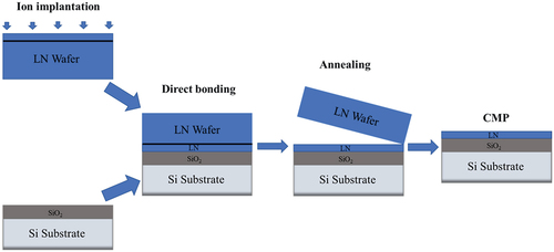
Figure 2. (a) The ring-down measurement of the ultra-high Q microcavity [Citation39], exhibiting an intrinsic Q factor of 1.23 × 10⁸. Inset: the scanning electron microscope (SEM) image of the microdisk, where the scale bar is 200 μm. (b) SEM image of the monolithic microring [Citation41]. (c) Photograph of an array of 1960 MZIs patterned in a 4-inch wafer. (d) Micrograph of unbalanced MZI. Inset: zoom-in micrographs of 1×2 multi-mode interferometer (MMI) and Euler bend waveguide [Citation38].
![Figure 2. (a) The ring-down measurement of the ultra-high Q microcavity [Citation39], exhibiting an intrinsic Q factor of 1.23 × 10⁸. Inset: the scanning electron microscope (SEM) image of the microdisk, where the scale bar is 200 μm. (b) SEM image of the monolithic microring [Citation41]. (c) Photograph of an array of 1960 MZIs patterned in a 4-inch wafer. (d) Micrograph of unbalanced MZI. Inset: zoom-in micrographs of 1×2 multi-mode interferometer (MMI) and Euler bend waveguide [Citation38].](/cms/asset/545c91e2-529d-4a92-a4f8-03d8e7acfbf0/tapx_a_2322739_f0002_oc.jpg)
Figure 3. (a) Photography of 8-inch wafer during DUV lithography. (b) Optical micrograph of a spiral LNOI waveguide with a length of 11.49 cm [Citation45]. (c) The illustration of the fabrication of thin-film PPLN waveguide [Citation46]. (d) The optical micrograph of the waveguides and periodic poled domains [Citation43].
![Figure 3. (a) Photography of 8-inch wafer during DUV lithography. (b) Optical micrograph of a spiral LNOI waveguide with a length of 11.49 cm [Citation45]. (c) The illustration of the fabrication of thin-film PPLN waveguide [Citation46]. (d) The optical micrograph of the waveguides and periodic poled domains [Citation43].](/cms/asset/de61352a-492f-4eb8-b349-1fdd7e93b9c1/tapx_a_2322739_f0003_oc.jpg)
Table.1. Comparison of different fabrication methods in terms of the-state-of-the-art propagation losses, loaded Q factors, minimum feature sizes, and integration scales, available by each method.
Figure 4. (a) Illustration of the growth of erbium ion doped bulk LN crystal [Citation74]. (b) Schematic of the fabrication of passive and active LNOI photonics by stitching and nanostructuring [Citation75].
![Figure 4. (a) Illustration of the growth of erbium ion doped bulk LN crystal [Citation74]. (b) Schematic of the fabrication of passive and active LNOI photonics by stitching and nanostructuring [Citation75].](/cms/asset/eb5c5e5b-2185-441d-9b11-fa6d8beafab3/tapx_a_2322739_f0004_oc.jpg)
Figure 5. (a) LNOI modulator with regular coplanar waveguides, with a Vπ of 1.4V and an EO bandwidth of 45 GHz [Citation103]. (b) Advanced LN IQ modulators [Citation104]. (c) Integrated LNOI modulators with capacity-loaded travelling electrodes and quartz substrate [Citation105].
![Figure 5. (a) LNOI modulator with regular coplanar waveguides, with a Vπ of 1.4V and an EO bandwidth of 45 GHz [Citation103]. (b) Advanced LN IQ modulators [Citation104]. (c) Integrated LNOI modulators with capacity-loaded travelling electrodes and quartz substrate [Citation105].](/cms/asset/37887ec5-05dd-4163-9687-4cd63ddcc512/tapx_a_2322739_f0005_oc.jpg)
Figure 6. (a) LNOI dual-polarization in-phase quadrature (DP-IQ) modulator integrated with an on-chip polarization rotator and combiner (PRC) [Citation116]. (b) Modulator with folded MZMs incorporating meander traveling wave electrode and optical waveguides [Citation118]. (c) Wafer-scale low-loss lithium niobate photonic integrated circuits [Citation44].
![Figure 6. (a) LNOI dual-polarization in-phase quadrature (DP-IQ) modulator integrated with an on-chip polarization rotator and combiner (PRC) [Citation116]. (b) Modulator with folded MZMs incorporating meander traveling wave electrode and optical waveguides [Citation118]. (c) Wafer-scale low-loss lithium niobate photonic integrated circuits [Citation44].](/cms/asset/b4c84409-f022-49fd-8707-7d76d390a700/tapx_a_2322739_f0006_oc.jpg)
Figure 7. MPM second harmonic generation. (a) the two MPM points at 1379.4 nm and 1381.5 nm, the inset figures are the electric profiles of the SH modes [Citation132] (b) the theoretical NCE values versus the relative thicknesses of LN layer [Citation132]. (c) the sketch of ridge waveguide in double-layer LNOI with reversed polarization [Citation133]. (d) Measured SHG spectrum of dual-layer ridge waveguide at room temperature, the inset figure shows the SHG power as a function of the pump power [Citation133].
![Figure 7. MPM second harmonic generation. (a) the two MPM points at 1379.4 nm and 1381.5 nm, the inset figures are the electric profiles of the SH modes [Citation132] (b) the theoretical NCE values versus the relative thicknesses of LN layer [Citation132]. (c) the sketch of ridge waveguide in double-layer LNOI with reversed polarization [Citation133]. (d) Measured SHG spectrum of dual-layer ridge waveguide at room temperature, the inset figure shows the SHG power as a function of the pump power [Citation133].](/cms/asset/f0f8a94a-6dc7-4529-affe-47a16c253187/tapx_a_2322739_f0007_oc.jpg)
Figure 8. Broadband SHG signals and tunable SHG laser. (a) Measured (black) and theoretical (blue) SHG transfer function for nanophotonic PPLN waveguide, broader than the bulk PPLN (orange) waveguide [Citation134]. (b) Measured broadening of birefringence phase matching spectra at different temperature gradients [Citation135]. (c-d) temperature sensitive SHG laser [Citation136,Citation137].
![Figure 8. Broadband SHG signals and tunable SHG laser. (a) Measured (black) and theoretical (blue) SHG transfer function for nanophotonic PPLN waveguide, broader than the bulk PPLN (orange) waveguide [Citation134]. (b) Measured broadening of birefringence phase matching spectra at different temperature gradients [Citation135]. (c-d) temperature sensitive SHG laser [Citation136,Citation137].](/cms/asset/2d8481fc-052f-46cc-b8cb-5eee45270121/tapx_a_2322739_f0008_oc.jpg)
Table 2. Comparison of SHG conversion efficiencies in peridically poled LNOI waveguide devices.
Figure 9. Kerr frequency combs based on LNOI (a) soliton crystals with different soliton numbers [Citation153]. (b) single-soliton and wo-soliton microcombs with near-octave soliton bandwidth [Citation154]. (c) (d) the soliton spectrum and step in a ytterbium-doped lithium-niobate microring [Citation155]. (e) Measurement scheme and optical spectrum of pulse-pumped Kerr frequency combs [Citation156].
![Figure 9. Kerr frequency combs based on LNOI (a) soliton crystals with different soliton numbers [Citation153]. (b) single-soliton and wo-soliton microcombs with near-octave soliton bandwidth [Citation154]. (c) (d) the soliton spectrum and step in a ytterbium-doped lithium-niobate microring [Citation155]. (e) Measurement scheme and optical spectrum of pulse-pumped Kerr frequency combs [Citation156].](/cms/asset/3ebf2360-3f59-456d-96b4-c5970ad50185/tapx_a_2322739_f0009_oc.jpg)
Figure 10. (a) EO comb generated by two coupled resonators for effective spectrum broadening [Citation162]. (b) Schematic of dual-comb spectroscopy for gas detection based on racetrack resonator [Citation163]. (c) Structure of power-efficient on-chip EO comb and combs with different pump wavelengths [Citation164]. (d) Structure of Mach-Zehnder modulator for visible-to-near-infrared electro-optic frequency combs [Citation165].
![Figure 10. (a) EO comb generated by two coupled resonators for effective spectrum broadening [Citation162]. (b) Schematic of dual-comb spectroscopy for gas detection based on racetrack resonator [Citation163]. (c) Structure of power-efficient on-chip EO comb and combs with different pump wavelengths [Citation164]. (d) Structure of Mach-Zehnder modulator for visible-to-near-infrared electro-optic frequency combs [Citation165].](/cms/asset/1cb512cc-f52c-4c4f-8cec-6a34aa414d8b/tapx_a_2322739_f0010_oc.jpg)
Figure 11. (a) High-rate quantum source realized by cavity enhanced SPDC on a micro-ring resonator [Citation186]. (b) Deterministic multi-photon generation scheme [Citation189]. (c) Integrated optical circuit for optical path coded photon state manipulation [Citation190]. (d) Integrated electro-optical frequency splitter for frequency domain manipulation [Citation191].
![Figure 11. (a) High-rate quantum source realized by cavity enhanced SPDC on a micro-ring resonator [Citation186]. (b) Deterministic multi-photon generation scheme [Citation189]. (c) Integrated optical circuit for optical path coded photon state manipulation [Citation190]. (d) Integrated electro-optical frequency splitter for frequency domain manipulation [Citation191].](/cms/asset/407befcf-8172-4e65-b4c2-71fc23a5134c/tapx_a_2322739_f0011_oc.jpg)
Figure 12. (a) LNOI-based superconducting nanowire single-photon detector [Citation97]. (b) LNOI-based low-noise upconversion SPD with off-chip silicon single-photon avalanche photodiode (SPAD) [Citation140]. (c) LNOI-based single photon buffer [Citation194]. (d) LNOI-based quantum memory [Citation195].
![Figure 12. (a) LNOI-based superconducting nanowire single-photon detector [Citation97]. (b) LNOI-based low-noise upconversion SPD with off-chip silicon single-photon avalanche photodiode (SPAD) [Citation140]. (c) LNOI-based single photon buffer [Citation194]. (d) LNOI-based quantum memory [Citation195].](/cms/asset/550b858e-d501-45f9-a553-fc1b1baec378/tapx_a_2322739_f0012_oc.jpg)
Figure 13. Single-frequency microlasers. (a) Coupled microrings [Citation199]. (b) Coupled microcavities consisted of a microdisk and a microring [Citation201]. (c) Single weakly perturbed microdisk laser from polygon modes [Citation202]. (d) Photograph of long-cavity length coupled microrings [Citation200]. (e) Optical graph of up-conversion fluorescence from Fabry-Perot resonator based on Sagnac loop reflectors [Citation203].
![Figure 13. Single-frequency microlasers. (a) Coupled microrings [Citation199]. (b) Coupled microcavities consisted of a microdisk and a microring [Citation201]. (c) Single weakly perturbed microdisk laser from polygon modes [Citation202]. (d) Photograph of long-cavity length coupled microrings [Citation200]. (e) Optical graph of up-conversion fluorescence from Fabry-Perot resonator based on Sagnac loop reflectors [Citation203].](/cms/asset/edfde1b5-41a0-4a79-a644-689414e665d7/tapx_a_2322739_f0013_oc.jpg)
Figure 14. (a) Schematic illustration of the integrated pockels laser [Citation84]. (b) Recorded laser frequency modulation rate for the increasing modulation speed [Citation84]. (c) Optical spectra of the dual-color lasing based on the SHG process [Citation84]. (d) Integrated schematic diagram of the ultrafast tunable laser [Citation220]. (e) False-colour SEM image of waveguide cross-section for a heterogeneously integrated Si3N4-LiNbO3 external cavity chip [Citation220]. (f) Point-cloud of the measured target scene in the three-dimensional optical ranging experiment [Citation220].
![Figure 14. (a) Schematic illustration of the integrated pockels laser [Citation84]. (b) Recorded laser frequency modulation rate for the increasing modulation speed [Citation84]. (c) Optical spectra of the dual-color lasing based on the SHG process [Citation84]. (d) Integrated schematic diagram of the ultrafast tunable laser [Citation220]. (e) False-colour SEM image of waveguide cross-section for a heterogeneously integrated Si3N4-LiNbO3 external cavity chip [Citation220]. (f) Point-cloud of the measured target scene in the three-dimensional optical ranging experiment [Citation220].](/cms/asset/67057adb-31ba-4c48-9ad1-b69ccf3d6b88/tapx_a_2322739_f0014_oc.jpg)