
Abstract
The current work attempts to provide a proof of concept for the achievement of semi-quantitative measurements by applying Surface Enhanced Raman Scattering (SERS) on thermally dewetted Au-films. In order to probe the anticipated advanced (device) material, Mitoxantrone (MTX) that exhibits strong SERS signal was utilized as a relevant prototype active molecular agent. The molecule was deposited on substrates of different morphology by spin coating and after evaluation of the collected SERS spectra it is shown that there is an almost linear correlation between the SERS intensity and the concentration of the SERS active molecule. In addition the enhancements achieved depend on the substrate’s morphology.
Introduction
Surface plasmon resonances associated with metallic nanostructures offer unique possibilities in several plasmonic applications such as Surface Enhance Raman Spectroscopy (SERS). Raman spectroscopy is the phenomenon arising from the inelastic scattering of light by molecular vibrations which are known to provide “fingerprint” information for molecular identification. The low scattering intensity of the phenomenon is a limiting factor for the technique when identification and quantification of molecules at very low concentrations is required. The latter can be overcome by using specifically designed plasmonic substrates upon which the molecules under investigation are deposited by some means. The local field enhancement offered by the substrates increases the Raman signal by orders of magnitude. Thus, SERS [Citation1] stands as one of the surface plasmon resonance techniques associated with metallic nanostructures able to offer unique possibilities.
Notably, the prevailing challenge for SERS is to achieve quantitative measurements in combination with identification of molecular species at extremely low concentrations. Within this concept, several works involving colloidal SERS substrates have already been reported [Citation2]. Colloidal substrates are in many cases preferable due to their ease of preparation and low cost with concurrent high enhancements. Besides, a number of works involve solid substrates which enable flexibility in sampling [Citation3].
Some of the early works on SERS active solid substrates involved flat surfaces covered with metallic films (of Ag or Au) with the metal forming nanoscale islands, achieved using appropriate deposition techniques [Citation4,5]. SEM, TEM, STM and AFM were employed in order to study the parameters of substrate preparation and investigate their correlation with the SERS signal that these substrates offer. The above mentioned works indicated that slowly deposited films produce higher SERS intensities than rapidly deposited films.
The metal deposition variables such as film nominal thickness, evaporation rate and substrate temperature have been studied for both metals, Au and Ag, by evaluating the resulting SERS enhancements. An increase in film thickness and the low evaporation rates were shown to upshift the wavelength at peak maximum of the plasmon resonances (λmax) and also increase the optical density of the substrates. In contrast, pre- and post-deposition annealing of gold films led to the formation of substrates that exhibited a downshift of λmax [Citation6].
The morphological parameters of silver nanostructured thin films prepared by sputtering on flat silicon (Si) substrates were correlated with their SERS activity. A maximum enhancement of the SERS signal has been found at the Ag percolation threshold, leading to the detection of a non-resonant Raman probe, at concentrations as low as 10−10 M, which corresponds to enhancement factors higher than 7 orders of magnitude [Citation7].
In the current work, Au films of various nominal thicknesses (<5 nm) were deposited by sputtering onto Si wafers <100>. The solid state thermal dewetting of Au films at 400 °C resulted in the formation of Au nanoparticles. As it has been shown [Citation8] the initial film thickness and the annealing details (temperature and heating time) control the resulting particle size distribution. Especially for ultrathin films, i.e. with nominal thickness <3 nm, annealing time does not severely influence the particle size distribution, while the Au nanoparticles always bear a spherical shape. The optical properties of the substrates were studied by UV-Vis spectroscopy and their enhancement on the Raman signal was evaluated by observing the Raman features of an active agent Mitoxantrone (MTX) that was properly spin coated on the substrates. The target of the work was to explore the ability of these “easy to prepare” substrates to accomplish quantification results. Our findings prove that under the methodology we applied for the deposition of the SERS active agent quantification results are feasible. Moreover, the detection limits achieved depend on sample’s morphology and at least for the samples studied become lower when the average diameter of the Au islands increase. Optimization of this process requires precisely engineered plasmonic properties of these substrates and will be the subject of a subsequent work.
Experimental
Preparation of substrates
Si wafers <100> (Ted Pella Inc.) were used as the substrates. Prior to Au deposition, Si chips 1 × 1 cm2 were cleaned by bath sonication with absolute ethanol. Gold was deposited onto the Si wafers by sputtering. Three substrate sets each with different morphology were prepared following the experimental conditions shown in Table . The table also includes details associated with the respective morphology. Each set includes four/five samples prepared with exactly the same experimental conditions. All substrates were subsequently annealed; temperature and time of annealing are designated in Table . Solid SERS substrates are easily reproduced, are quite fast prepared, with minimal requirements in consumables or/and additional substances, e.g. no need of aggregating agents typically used in colloidal substrates.
Table 1. Details concerning the SERS substrates and their preparation.
Deposition of SERS active substance
Mitoxantrone dihydrochloride (MTX) purchased from Sigma-Aldrich served as the SERS active molecule. Aqueous (3D water) solutions of MTX at several concentrations (0·5, 1, 1·5, 2, 10 μg ml−1) were prepared. In order to study the SERS response of the Au coated Si wafers, the MTX molecules were properly deposited on the relevant Au thin films, by spin coating 20 μL droplets of the different aqueous MTX solutions. The spin coating parameters were 2000 rev/min for 120 s.
Characterization of the substrates
The morphology of the Au coated Si wafers was studied by SEM – Zeiss SUPRA 35 VP-FEG equipped with EDS (Bruker GmbH, Quanta200) and BSE detectors (K E Developments, Ltd), operating at 5–20 keV. The plasmon resonances of the Au islands on each substrate were detected by UV-Vis spectroscopy (Hitachi U-3000 reverse optics spectrophotometer) operating at specular reflection mode.
SERS measurements
For the collection of the Raman spectra the 632·8 nm, 514·5 excitation wavelengths from a He–Ne laser (Optronics Technologies S.A. model HLA-20P, 20 Mw) and a DPSS laser (Cobolt FandangoTM, 150 mW) respectively were used. Laser power was kept at ~0·6 mW and was focused on sample by a 50× (NA = 0·55) microscope objective. The back-scattered radiation was collected and analyzed by the T-64000 Jobin Yvon (ISA-Horiba group) μRaman system using its single spectrograph configuration. The rejection of the elastic scattered photons was accomplished by appropriate edge filters (LP02-514RU-50 and LP02-633RU-50 RazorEdge® Long Wave Pass Filter, U grade 50 mm diameter). The Raman photons were dispersed by a 600 grooves/mm (76 mm × 76 mm) grating and detected by a standard LN2- cooled (140 K) Multi Phase Pinning, front-illuminated open electrode 1024×256 pixels CCD (Symphony® II, Horiba Scientific).
Results and discussion
Typical SEM images of the Au coated Si wafers after the annealing process is depicted in Figure . Gold islands can be clearly resolved in the images and are a consequence of the annealing process. Image processing using ImageJ software reveals the particle size distribution of the Au islands. A characteristic example of one of the samples with 1 nm nominal thickness of Au is shown in Figure (b). From the statistical analysis the average particle size is ~26 nm while the standard deviation is ~4·5 nm.
Figure 1. (a) SEM image of the annealed 1 nm nominal thickness Au-coated silicon wafer (26 nm average diameter). Dotted circle indicates approximately the size of the laser spot for Raman/SERS excitation. (b) Particle size distribution for the sample shown in (a). Average was performed on ~2000 particles. (c and d) SEM images of the <1 nm (5 nm) and 2 nm (104 nm) nominal thickness Au-coated silicon wafers respectively. Scaling bar appearing in (a) applies also on (c) and (d).
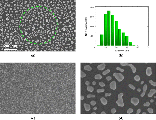
A note is made of the fact that the Raman back scattered light is collected from a large number of Au nanoparticles probed (Figure (a)), where aqueous solutions of the model compound were spin coated. On the other hand, it is also clear from the same SEM images that it is not possible to stimulate coupled plasmon resonance excitation, due to the largely spaced Au nanoparticles for hot-spot formation, at least for the annealed Au-coated Si wafers with 1 and 2 nm nominal thicknesses.
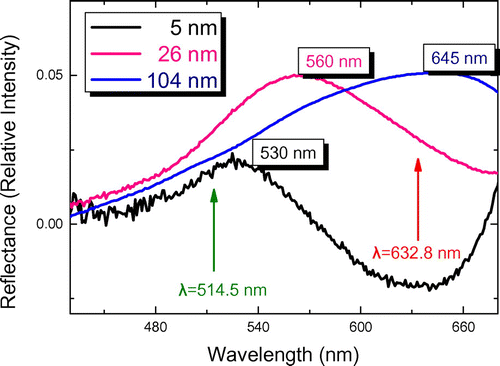
The Reflectance of the samples in the visible (Figure ) indicates that plasmon resonances of the Au islands do exist and the maximum of the corresponding peak depends on the average Au-island diameter. The two laser wavelengths used for the collection of the SERS spectra are denoted in the figure by arrows. The corresponding reflectance spectrum from the substrates before the annealing did not reveal any observable plasmon peaks.
Figure 2. Reflectance spectra in the visible spectral region from the silicon wafers with average particle diameter of 5, 26 and 104 nm. Arrows designate the wavelengths of the two lasers used for the collection of the SERS spectra.
Mitoxantrone is a synthetic chemotherapeutic agent with proven antitumor activity against several forms of cancer. The chemical formula of Mitoxantrone is shown on the upper right corner in Figure . Typical Raman spectra of MTX samples using the 632·8 nm excitation wavelength are characterized by severe fluorescence [Citation9] which masks all vibrational modes. On the contrary, SERS spectra of MTX are characterized by significant fluorescence depression and strong enhancement of the vibrational bands. Moreover, using this particular excitation wavelength the resonance Raman conditions are fulfilled, anticipating an additional factor for the enhancement of the inelastic light scattering intensities, in terms of Surface Enhanced Resonance Raman Scattering (SERRS).
Figure 3. SERS spectra recorded from the dewetted substrates with average Au-island diameter 26 nm. The spectra correspond to the five different concentrations of the solutions deposited on them. The SERS spectrum from a colloidal SERS substrate is plotted on top.
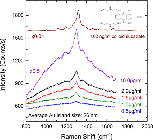
Raman spectra obtained from Au-free Si wafers as well as the ones that were Au-coated without thermal annealing did not exhibit any vibrational modes attributed to MTX, even for the case of the solution with the maximum concentration studied (10 μg ml−1).
SERS spectra were collected from three sets each of which consisted of five similar substrates. All parameters of sputtering and annealing were kept constant for each of the five substrates which led to the formation of Au islands with similar size distribution (as observed in the respective SEM images). The samples subjected to SERS analysis differed only on the portion of MTX deposited on each of them. For statistical purposes, a set of forty spectra was collected for each sample; each of these spectra was collected from different positions on the surface of the sample. The average spectrum for each of the five samples for the case of the set of substrates having 26 nm average diameter particles is given in Figure . The profile of these spectra is similar and matches the typical MTX SERS spectra obtained from colloidal substrates (top spectrum in Figure ) [Citation9,10]. Moreover, samples with different portion of MTX, spin-coated on them, exhibit different absolute intensities of their vibrational bands in the corresponding Raman spectra. The progressive increase of the SERS intensity, when increasing the concentration of MTX in the respective solutions used for the spin coating, signifies that under the procedures followed in our experiments SERS may be used in order to quantify MTX.
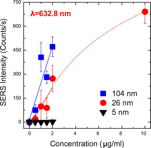
Figure depicts the average (from the ensemble of the forty spectra collected from each sample) SERS intensity of the characteristic 1300 cm−1 band as a function of MTX concentration in the solutions that were spin-coated on the Au-coated silicon wafers. Error bars correspond to the respective standard deviation. The main spectral feature of MTX is attributed to the ring stretch, eventually coupled with the aromatic carbonyl groups or/and with a significant contribution from C–N stretching. An almost linear correlation is observed between the SERS intensity and the concentration of the solution that was spin coated. The latter suggests that at least in the concentration range under investigation, semi-quantitative SERS measurements are feasible using thermally dewetted Au films sputtered onto Si wafers. Deviation from linearity is considered minimal at least up to the higher concentration studied (i.e. 10 μg ml−1 for the 26 nm sized Au-islands). The best detection limits are achieved for the substrates with ~104 nm average diameter of Au-islands. Moderate SERS intensities are observed for the substrates with ~26 nm average diameter Au-islands, while minimum intensities are recorded for the substrates with ~5 nm sized Au-islands. The best performance of the ~104 nm sized Au islands may be explained by the fact that the corresponding plasmon resonances of the substrates with this particular morphology, shown in Figure , are near the excitation wavelength (632·8 nm).
Figure 4. SERS intensity as a function of MTX concentration in the solution deposited on the dewetted Au-coated silicon wafers. Linear fits are shown up to 2 μg ml−1 while an estimated dotted curve is drawn towards the 10 μg ml−1 for the substrates with 26 nm sized Au-islands.
Considerably low SERS intensities are recorded from all substrates when the 514·5 nm excitation wavelength is used rendering quantification inapplicable. The latter may be explained by the fact that for this specific excitation wavelength no resonance Raman conditions are expected for MTX. This is better supported by the low intensities recorded even for the substrates with ~5 nm average diameter Au-islands which exhibit plasmon resonance at 530 nm.
Plasmonic engineering of the Au islands by variation of the thermodynamic parameters that control the size of the islands and their morphology in general, may be valuable in order to optimize the process i.e. obtain maximum SERS signal thus minimizing the detection limits reached.
Conclusions
A methodology that enables SERS quantification measurements using thermally dewetted Au-islands is proposed. Mitoxantrone was used as a SERS active agent and was deposited on the dewetted surfaces after spin coating specific volume of its aqueous solutions possessing different concentrations. For statistical purposes, Raman spectra were selected from forty different locations on the sample’s surface. The calculated average intensity of the characteristic Raman band of MTX was found to depend almost linearly on the spin-coated solution’s concentration, a fact that strongly supports that the methodology proposed enables SERS quantitative measurements. The morphology of the dewetted surfaces may be triggered in order to optimize the proposed methodology.
Disclosure statement
No potential conflict of interest was reported by the authors.
References
- Le Ru EC, Etchegoin PG. Principles of surface-enhanced Raman spectroscopy and related plasmonic effects. Amsterdam: Elsevier; 2009.
- Anastasopoulos JA, Beobide AS, Sygellou L, et al. Surface-enhanced Raman scattering of pyridine-functionalized multi-walled carbon nanotubes. J Raman Spectrosc. 2014;45(6):424–430.10.1002/jrs.v45.6
- Kämmer E, Olschewski K, Bocklitz T, et al. A new calibration concept for a reproducible quantitative detection based on SERS measurements in a microfluidic device demonstrated on the model analyte adenine. Phys Chem Chem Phys. 2014;16(19):9056–9063.10.1039/c3cp55312d
- Schlegel VL, Cotton TM. Silver-island films as substrates for enhanced Raman scattering: effect of deposition rate on intensity. Anal Chem. 1991;63(3):241–247.10.1021/ac00003a010
- Dawson P, Alexander KB, Thompson JR, et al. Influence of metal grain size on surface-enhanced Raman scattering. Phys Rev B. 1991;44(12):6372–6381.10.1103/PhysRevB.44.6372
- Sockalingum GD, Beljebbar A, Morjani H, et al. Characterization of island films as surface-enhanced Raman spectroscopy substrates for detecting low antitumor drug concentrations at single cell level. Biospectroscopy. 1998;4(S5):S71–S78.10.1002/(ISSN)1520-6343
- Santoro G, Yu S, Schwartzkopf M, et al. Silver substrates for surface enhanced Raman scattering: correlation between nanostructure and Raman scattering enhancement. Appl Phys Lett. 2014;104(24):243107.10.1063/1.4884423
- Govatsi K, Chrissanthopoulos A, Dracopoulos V, et al. The influence of Au film thickness and annealing conditions on the VLS-assisted growth of ZnO nanostructures. Nanotechnology. 2014;25(21):215601.10.1088/0957-4484/25/21/215601
- Manikas AC, Beobide AS, Voyiatzis GA. Quantitative analysis by surface enhanced Raman scattering utilizing an oscillating-cell and right angle collection geometry. Analyst. 2009;134(3):587–592.10.1039/B815053B
- Anastasopoulos JA, Beobide AS, Voyiatzis GA. Quantitative surface enhanced Raman scattering measurements at the early stage of active agent release processes. J Raman Spectrosc. 2013;44(3):401–405.10.1002/jrs.v44.3