
 ?Mathematical formulae have been encoded as MathML and are displayed in this HTML version using MathJax in order to improve their display. Uncheck the box to turn MathJax off. This feature requires Javascript. Click on a formula to zoom.
ABSTRACT
Ultrafast electron microscopy (UEM) has a broad scope of application across material systems and scientific disciplines. In UEM, we investigate multiscale dynamics in the spatial domain ranging from micrometres to ångströms, in reciprocal space, and on timescales from microseconds to attoseconds, with an energy resolution of a few electronvolts or less. Notably, UEM has played a pivotal role in visualisation of ultrafast structural dynamics with high local selectivity, enabling the exploration of the dynamic nature of chemical bonding in non-equilibrium states and investigation of electron – photon interactions to manipulate free-electron wavefunctions. This breakthrough has created new opportunities in condensed matter physics, chemical dynamics, and quantum electrodynamics. In addition, efforts are underway to achieve high-resolution UEM in correlative real-space microscopy to diffractography and spectroscopy in a single instrument for comprehensive investigations of light – matter interactions and structure – dynamics – function relations. In this review, we provide an overview of the current state of UEM imaging capabilities and scientific interests, outlining the technological challenges faced by UEM in related fields and exploring potential approaches to overcome these challenges. Furthermore, we highlight the emerging fields of interest and present future perspectives that can further extend the imaging capabilities of UEM.
1. Introduction
Revealing accurate structures at the atomic level is the cornerstone for understanding a myriad of physical, chemical, material, and biological phenomena. To unravel the equilibrium structures from individual molecules to macromolecules and solids, an array of well-established experimental techniques are employed, including X-ray and neutron diffraction [Citation1–3], NMR [Citation4], and electron microscopy [Citation5–11].
The structure of matter is not static but dynamic. This is related to the extent of change relative to the timescale. Structural changes occur over extended timescales, during which various sequential steps are integrated when measured in the steady state. For instance, the formation and breaking of chemical bonds occur on the timescale of a single vibrational period, i.e., tens to hundreds of femtoseconds, on a length scale of ångström [Citation12]. In the assemblies of atoms and molecules, localised processes involving electron – phonon and phonon – phonon interactions occur within a few to tens of picoseconds [Citation13–16]. Subsequent collective nuclear events, such as acoustic phonon generation, strain/heat propagation, and structural phase/conformational changes, evolve over a longer duration, ranging from picoseconds to milliseconds, depending on the spatial scale of the change [Citation17–19].
A series of approaches have been developed for the transient structural characterisation at atomic and molecular timescales. Time-resolved diffraction/scattering techniques, using both X-rays and electrons, offer ultrafast temporal resolution. This allows direct observation of the changing nuclear configurations in molecules and solids upon pulsed perturbation, in reciprocal space, thus on an ensemble scale [Citation20–25]. To obtain details on the non-periodic structural entities and characteristics of individual particles at the nanoscale, we must employ structural-probing techniques with local selectivity and ultimately, atomic spatial resolution. Moreover, accessibility poses another challenge, particularly when utilising time-resolved X-ray diffraction/scattering, which is set up only in large accelerator facilities [Citation26–30].
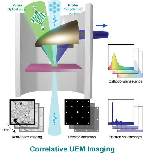
Consequently, recent efforts have been channelled toward developing and modifying tabletop transmission electron microscopes (TEMs) with laser-driven photocathodes, termed as ultrafast electron microscopy (UEM), to record micrographs with the spatial and temporal resolutions of TEM and ultrafast spectroscopy, respectively. In UEM, femtosecond laser pulses excite a specimen and illuminate the photocathode to generate a pulsed electron beam synchronised to the excitation pulse (). The optical-pump and electron-probe pulses are cycled until a time-resolved micrograph, diffractogram, or electron energy-loss (EEL) spectrum at a time delay (Δt) between the pump and probe is built with an acceptable contrast or a signal-to-noise ratio. The entire procedure is repeated while Δt is scanned to cover a dynamic range of interest, analogue to the pump-probe stroboscopic scheme in ultrafast spectroscopy [Citation31].
Figure 1. Schematic overview of high-resolution correlative imaging in UEM. (left) experimental setup illustrating the standard operation of ultrafast electron microscopy (UEM) equipped with optical pump and electron probe for stroboscopic measurements. UEM offers correlative capabilities for ultrafast imaging, diffractography, electron energy-loss (EEL), and cathodoluminescence (CL) spectroscopies. In this configuration, femtosecond (fs) ultraviolet laser pulses are directed at photocathodes to generate pulsed photoelectrons, which are synchronized in time and overlapped in space with the pump pulses applied to the specimen to initiate photoinduced dynamics. UEM provides multimodal imaging capabilities that enable complementary mapping of structural, electronic, and chemical dynamics at the nanoscale. (right) for ultrafast real-space imaging and diffractography in reciprocal space, UEM allows visualization of nanoscale morphological changes, such as warping or strain wave propagation, as well as lattice thermalization or vibrations at the ångström scale, providing direct evidence of the object’s structural motion. The exploration of the light-induced electric-field enhancement and non-equilibrium magnetic or spin states can be observed through the electron – matter interactions, taking advantage of the spatiotemporal accessibility of the electron probe to the intrinsic length and timescales of material dynamics. To gain a thorough understanding of concurrent electronic-transition dynamics in consistent measurement, ultrafast EEL and CL spectroscopies serve as complementary techniques in UEM, enabling the measurement of valence and core-level dynamics with single-particle selectivity. The advantageous capabilities of energy-filtered and -selected mapping of nanoparticles or grains are particularly valuable for visualizing the time-resolved evolution of chemical states, molecular bonding configurations, and charge-carrier transport behaviour in real time, at the nanometre scale. The integration and realization of these diverse imaging modalities in UEM hold the promise of unlocking new insights and enabling a deeper understanding of ultrafast structural and electronic dynamics at their relevant scales, while also revealing their spatiotemporal correlations.

The early development on stroboscopic imaging in TEM began in the 1970s, through the contributions of Bostanjoglo and Rosin [Citation32,Citation33]. Following the pioneering contribution of Zewail to UEM at California Institute of Technology [Citation34], almost a dozen groups worldwide joined research focusing on UEM applications, located in China [Citation35], France [Citation36], Germany [Citation37,Citation38], Israel [Citation39], Japan [Citation40], Korea [Citation41], Saudi Arabia [Citation42], Sweden [Citation43], Switzerland [Citation44,Citation45], and the United States [Citation46–48] (listed in alphabetical order). These groups have demonstrated that UEM has promising applications in various fields, including the investigation of lattice motions in nanostructures [Citation49–51], near-field imaging of electron – photon interactions [Citation44,Citation52–54], quantum manipulation of free electron wavefunctions [Citation55,Citation56], photoacoustic strain waves and mechanical motions of two-dimensional materials and nanomaterials [Citation57–59], phase transformations in correlated systems [Citation54,Citation60,Citation61], and charge-carrier dynamics [Citation62]. As a complementary technique, single-shot imaging for capturing the irreversible transition of a material, established by Dömer and Bostanjoglo in 2003 [Citation63], was refined to dynamic TEM by Campbell and Browning at the Lawrence Livermore National Laboratory, with resolutions on the scales of tens of nanometres and tens of nanoseconds [Citation64,Citation65]. When UEM is operated in scanning mode and detects back-scattered electrons, it offers a distinct way to observe surface-sensitive photoinduced charge-carrier dynamics based on changes in secondary electron emission [Citation66–69].
In present UEM, the utilisation of femtosecond-pulsed electron probes has been widely restricted to low-magnification imaging on a micrometre-scale field of view or electron diffractometry, while the capacity for imaging at higher magnifications has largely been confined to temporal resolutions within the nanosecond range. The conflicts in the spatiotemporal and energy resolutions of UEM originate from the Coulomb repulsion between the charged particles, i.e., electrons in the imaging pulsed beam, which are confined in space and thus also in time. This repulsion becomes significantly stronger in dense beams such as femtosecond-duration photoelectron packets [Citation70–74]. Coulomb effects broaden the electron pulses spatially and temporally. To overcome the pulse broadening, several strategies have been discussed, including reducing the excess energy above the work function of the photocathode [Citation71], modifying the geometry of the photocathode [Citation43], employing a reflectron, i.e., a time-of-flight electrostatic mirror capable of reversing the chirp [Citation75–77], and applying ponderomotive deflection [Citation78,Citation79]. Alternatively, when radiofrequency (RF), microwave, and terahertz (THz) electric fields are applied to pulsed electron packets of energy (therefore temporal) distribution, lagging electrons at the tail of the pulse are accelerated, whereas leading electrons at the front are decelerated, resulting in the compression of the initial pulse [Citation80–86]. However, these pulse compression schemes require a complete redesign of the UEM apparatus, which is beyond the scope of condensed-matter physicists.
To circumvent the abovementioned technological challenges, the gun region has been optimised to generate photoelectron packets with the minimal space-charge effects and limit the number of photoelectrons in each femtosecond-duration pulse to a few dozen or less in a (quasi-)single-electron regime [Citation49,Citation87,Citation88]. To obtain an image of acceptable quality in seconds and register at least tens of electrons per pixel on a conventional charge-coupled device (CCD) camera, a stroboscopic measurement with a repetition rate of ≥1 MHz is desired. However, this high repetition rate restricts the choice of specimens because they must fully revert to their original configurations in less than 1 µs, which is practically very rare. To fully utilise UEM, as originally intended for spatiotemporal imaging, the intertwined issues of pulse broadening and repetition rate must be addressed.
Owing to the inherent constraints related to electron probing and existing technological challenges that remain unresolved, investigations involving time-resolved imaging, diffraction, and electron energy-loss spectroscopy (EELS) in UEM have primarily been conducted separately. For example, time-resolved EELS can provide insights into the intraband and interband dynamics of valence electrons [Citation89–91]. However, when performed in an ultrafast electron microscope optimised for time-resolved imaging and diffraction, the energy resolution of photoelectrons typically exceeds 1 eV. This limits the attainable information regarding the characteristics and behaviour of reactive valence electrons embedded within a few electronvolts. Despite the inherent limitations that require technological advancements, UEM using a single tabletop instrument can serve as an effective correlative apparatus that encompasses multiple probing domains in space, time, and energy. This potential can be fully harnessed once high spatiotemporal and energy resolutions are realized simultaneously. By synergistically integrating time-resolved diffraction and EELS with direct imaging in real space, UEM can be repositioned as a robust platform for imaging ultrafast phenomena (). This allows a thorough exploration of structural dynamics, spanning from ångströms to micrometres, which can subsequently be correlated with concurrent electronic transitions and chemical reactions occurring at corresponding spatial and temporal scales.
In this short review, we focus on exploring recent advancements, the present technological landscape, and the emerging scientific interest in UEM to support the pursuit of realizing correlative imaging. We survey the latest efforts to overcome these challenges towards realizing more practical measurements that move beyond mere instrumental advances. We then highlight the achievements in time-resolved real-space imaging, aiming to uncover potential opportunities for future correlative investigations involving electron diffraction and EELS as well as their scientific significance. We also discuss the inherent methodological and technological difficulties associated with the use of photoelectron probes. Finally, we outline prospective directions for real-space imaging in UEM.
2. Applications and opportunities of correlative imaging in UEM
In this section, we offer a summary of studies using UEM, focusing particularly on its role in time-resolved real-space imaging, from its inception to present-day research. We first explore correlative measurements that employ time-resolved electron diffraction and EELS to probe the complex structural and electronic dynamics of nanoscale solid-state materials. We also discuss the current advancements and potential future directions of correlative UEM imaging.
2.1. Earlier studies on imaging and correlative measurements in UEM
In the early stages, time-resolved imaging in UEM, led by the Zewail research group, was used to visualise the mechanical motions of diverse micro- and nanostructures photoexcited with nanosecond-duration pulses. The structures observed in these studies include graphite films [Citation92], biomolecules [Citation93,Citation94], crystal beams [Citation95], nanoscale cantilevers [Citation96,Citation97], and molecular crystals [Citation98] (). These investigations particularly emphasised the observation of photoinduced dynamics encompassing spatial and temporal dimensions. The displacements and oscillatory behaviour of nanomechanical motions, such as nanodrumming [Citation92], have been resolved at the nanometre scale in real space. These studies established the foundation for utilising UEM in time-resolved real-space imaging, facilitating the investigation of the morphological and structural dynamics of various materials.
Figure 2. Nanosecond real-space imaging in UEM. a. Four-dimensional imaging of nanomechanical motions. 2D projected images of multiwalled carbon nanotube at the representative time delay and 3D reconstructed image of transient motion. b. Time-resolved bright-field and dark-field imaging and electron diffraction of spin-crossover phase transition and morphology dynamics in a metal-organic framework nanoparticle. Part a reprinted with permission from [Citation96], American Association for the advancement of science. Part b adapted with permission from [Citation99], Springer Nature.
![Figure 2. Nanosecond real-space imaging in UEM. a. Four-dimensional imaging of nanomechanical motions. 2D projected images of multiwalled carbon nanotube at the representative time delay and 3D reconstructed image of transient motion. b. Time-resolved bright-field and dark-field imaging and electron diffraction of spin-crossover phase transition and morphology dynamics in a metal-organic framework nanoparticle. Part a reprinted with permission from [Citation96], American Association for the advancement of science. Part b adapted with permission from [Citation99], Springer Nature.](/cms/asset/3577fbaa-1dd0-4fba-9d10-2024208feba9/tapx_a_2316710_f0002_oc.jpg)
UEM has expanded its capabilities in imaging the structural dynamics of correlated electron systems, as exemplified in the investigations involving particle-dependent photoinduced insulator-to-metal transitions in VO2 [Citation100] and spin-crossover dynamics in metal-organic framework nanoparticles () [Citation99]. A combination of time-resolved real-space imaging and diffraction was used for these measurements. The real-space imaging was employed for filming the changes in diffraction contrasts of individual nanoparticles associated with the phase transitions and morphological dynamics. Simultaneously, the crystallographic changes in these nanoparticles, including orientation and symmetry, were evaluated based on the time-dependent variations in diffraction peak intensities and spacings. This integrated approach allowed for a comprehensive analysis of both the structural and dynamic aspects at fundamental length scales. However, the probing timescale was limited by the nanosecond-duration pulses employed, during which both the electrons and lattices already reach thermal equilibrium. Consequently, the ultrafast structural dynamics associated with the non-equilibrium interplay among electrons, spins, phonons, and lattices that occur on femtosecond to picosecond timescales was veiled.
Owing to technological progress in femtosecond laser systems, UEM has concurrently advanced to achieve femtosecond temporal resolution. It is possible to visualise the phase transition of VO2 in real time with a temporal resolution of approximately 3 ps, operating in the regime of single electron per pulse at a repetition rate of 80 MHz [Citation88]. However, this repetition rate provides a relaxation time of only 12.5 ns between successive pump pulses. Consequently, the photoinduced diffraction-contrast changes in the VO2 nanoparticles, resulting from the phase transition, were not fully measured as heat accumulation persisted; only a few particles showing reversible changes were captured. This is an example that calls for employing lower repetition rates for such measurements using different types of femtosecond laser systems, while reducing the space-charge effects and compensating for the low signal-to-noise ratio of the tailored photoelectron pulses. The transient deformation of a gold nanofilm was successfully visualised by examining the time-dependent alterations in the bend contours of the film at a comparatively low repetition rate of 200 kHz [Citation101]. The corresponding changes in the Bragg spot intensity and position in the diffraction patterns provide additional evidence of the ultrafast response of the local crystal lattice.
While there have been various correlative UEM imaging studies, which combine imaging and diffraction techniques, time-resolved EELS has mainly been conducted alone [Citation89,Citation102,Citation103]. This is because of the distinguished properties of the probing electron beam necessary for conducting EELS. Time-resolved EELS requires space-charge-free conditions to realize a sufficiently high energy resolution (≤1 eV) for discerning spectral features, primarily at core-loss regions (>50 eV), which contain element-specific chemical information. In these spectral regions, the count of probing electrons decrease exponentially due to the scattering cross-section of impinging electrons, which diminishes inversely with the increase in energy loss. Therefore, time-resolved EELS must be operated at a high laser repetition rate or by applying nanometric photocathodes to reduce the beam emittance and increase the coherence and energy resolution. These prerequisites make it difficult to uniformly apply the same experimental conditions for both imaging and diffraction. However, in low-loss regions (<50 eV), the time-resolved EELS in UEM successfully tracked photoinduced plasmon oscillations in graphite with temporal and energy resolutions of hundreds of femtoseconds and 1 eV, respectively [Citation90]. In this study, the changes in the dielectric properties of the plasmon resonances and electronic structure were attributed to atomic displacement motions. These motions would not have been revealed without the aid of time-resolved crystallography, which is structurally sensitive at the lattice level. Therefore, the crucial factor for maximising the capabilities of UEM and unlocking new scientific opportunities in related areas corresponds to addressing the technological challenges involved in establishing correlations between the electronic and structural dynamics within a single instrument. In this sense, it is ultimately desired to operate UEM in the (quasi-)single-electron regime, which eliminates the detrimental space-charge effects on the resolutions in space, time, and energy. However, this often conflicts with low repetition rates of the stroboscopic measurements. This represents a challenging step in advancing UEM for wider applications.
2.2. Recent applications of time-resolved imaging in UEM
Recent progress in lasers, electromagnetic optics, specimen holders, nanofabrication technologies, and detectors for electron microscopy has transformed UEM into a viable platform for exploring a wide range of low-dimensional and strongly-correlated materials at the nanoscale. The simultaneous spatiotemporal and energy resolutions of UEM enable the investigation of cooperative behaviours in these materials. Such investigations focus specifically on electron-spin-phonon-lattice-morphology correlations in their characteristic temporal scope, which ranges from attoseconds to femtoseconds and even extends to microseconds, depending on the spatial length scale. Currently, some of the active UEM research fields involve the direct visualisation of photoinduced phase transitions [Citation60,Citation61], strain – wave dynamics in two-dimensional materials and nanoscale metallic objects [Citation50,Citation104,Citation105], real-space imaging of charge-diffusion dynamics [Citation106], and Lorentz microscopy [Citation107,Citation108]. This can be realized by leveraging the exceptional sensitivity of the electron beam to crystallographic changes directly reflected in time-framed dark-field (DF) and bright-field micrographs.
Ultrafast DF imaging in UEM has been utilized for observing the phase-transition dynamics of the photoinduced charge density wave (CDW) in 1T-TaS2 at spatiotemporal resolutions of 5 nm and 200 fs [Citation61]. The ultrafast CDW dynamics have been extensively investigated with dedicated ultrafast electron diffractometry for its direct access to crystallographic information [Citation109,Citation110]. The photoinduced transition from a nearly commensurate phase at low temperatures to an incommensurate phase at higher temperatures involves melting of the superlattices. This in turn leads to the loss of satellite reflections in diffractograms. To elucidate the structural evolution in real space during the ultrafast transition, satellite diffraction peaks were used to construct DF micrographs using a specially designed objective lens aperture that exclusively permitted these peaks to constitute the back focal plane. Time-framed DF micrographs were obtained by selectively visualising the CDW domains via distinct diffraction contrasts and revealing their evolution and relaxation (). Notably, this study employed a high repetition rate of approximately 400 kHz and used a distinctive specimen configuration with a gold film. This design reflected the majority of the pump beam, leaving only the irradiation area of less than 2 2 µm2 exposed, promoting efficient heat dissipation. This study illustrates that by developing unique imaging methods and specimen configurations, high-resolution imaging of correlated phenomena at small spatial dimensions and femtosecond scales can be achieved. Such advancements will further our understanding of intricate interactions between electrons and lattices, as well as their structural correlations within macroscopic domains.
Figure 3. Recent applications in ultrafast imaging in UEM. a. (left) ultrafast dark-field imaging of CDW dynamics. (right) schematic illustration of the specimen preparation for efficient heat dissipation. b. Nanoscale vibrational dynamics of a gold nanoprism observed in dark-field ultrafast imaging. c. Ultrafast imaging of charge carriers in charge-dynamics electron microscopy. Spatiotemporal evolution of the reconstructed charge density in InAs crystal. Part a adapted with permission from [Citation61], American Association for the advancement of science. Part b adapted with permission from [Citation50], Springer Nature. Part c adapted with permission from [Citation106]. Copyright 2023 American Chemical Society.
![Figure 3. Recent applications in ultrafast imaging in UEM. a. (left) ultrafast dark-field imaging of CDW dynamics. (right) schematic illustration of the specimen preparation for efficient heat dissipation. b. Nanoscale vibrational dynamics of a gold nanoprism observed in dark-field ultrafast imaging. c. Ultrafast imaging of charge carriers in charge-dynamics electron microscopy. Spatiotemporal evolution of the reconstructed charge density in InAs crystal. Part a adapted with permission from [Citation61], American Association for the advancement of science. Part b adapted with permission from [Citation50], Springer Nature. Part c adapted with permission from [Citation106]. Copyright 2023 American Chemical Society.](/cms/asset/ddb55ee6-58d2-4bf2-af26-8ccb599295a9/tapx_a_2316710_f0003_oc.jpg)
Strain waves and coherent photoacoustic phonon dynamics in two-dimensional materials have been an area of intense research in UEM. High sensitivity of the electron beam to lattice distortions makes it advantageous for imaging strained or distorted structures. UEM has enabled spatiotemporally resolving the propagation and relaxation of coherent acoustic phonons launched by various features such as flake edges [Citation111,Citation112], lattice imperfections [Citation113], and CDW [Citation40] in transition metal dichalcogenides such as TaS2 and MoS2. Through these measurements, strain wave modes, with oscillation frequencies ranging from megahertz to terahertz, were resolved. Nanometre-scale phonon responses of anisotropic intra-/interlayer strain waves were also measured and correlated with the crystallographic orientation, local thickness differences, and defect-concentration-dependent delay in the launch of oscillations owing to the sub-picosecond and nanometre resolutions in UEM. DF imaging is more effective in visualising acoustic vibrational motions in nanoparticles [Citation49,Citation50]. The interactions between the nanoparticles and substrate, as well as the transient structural deformation effects on the phonon responses, were investigated (). Recent study on the DF imaging of anisotropic bulging dynamics in black phosphorus membranes demonstrated the capability to visualise distinct lattice motions that rely on crystalline axes and nanomechanical properties at nanosecond resolution [Citation114].
Charge-dynamics electron microscopy has been performed to elucidate the spatiotemporal evolution of electronic structures and their correlative behaviours in solid-state materials. It enables mapping of femtosecond dynamics of charge carriers and plasma [Citation106,Citation115]. Imaging relies on the generation of THz near fields resulting from spatial disparities in the diffusion of carriers between holes and electrons. The ultrafast electron beam interacts inelastically with the THz near fields, inducing kinetic energy distributions of the electrons in the pulse. By reconstructing the spatiotemporally-resolved energy of the electron probe, the phase and amplitude of the THz near field on InAs were mapped (see ) [Citation106]. By integrating the high space and energy resolutions of cathodoluminescence (CL), UEM can also access photoinduced charge-transport dynamics in photovoltaic systems. This will facilitate the establishment of connections between charge-carrier diffusion, recombination kinetics, and dynamic local structural properties such as lattice strain and atomic vacancies. These factors come into play on the corresponding timescales, giving rise to various processes, including nonradiative decay through phonons, energy dissipation via the launch of incoherent strain waves, and transient domain formation. Time-resolved Lorentz electron microscopy has led to new avenues for the imaging of photoinitiated magnetic fields [Citation107]. This can reveal the photothermally-induced life cycle of magnetic skyrmions, which are particle-like topological magnetic textures. These pursuits can aid in understanding the structural and electronic/spintronic origins that govern fundamental, ultrafast phenomena. Furthermore, they are pivotal for fine-tuning the functionality of materials and optimising device operations.
Correlative imaging in UEM is synergistic with other advanced TEM techniques; for example, UEM can be combined with in-situ methods to explore photoinduced dynamics in soft matter. This can elucidate ultrafast molecular interactions within liquid or cryogenic environments, including phenomena such as the breaking and formation of chemical bonds on the femtosecond scale. This approach can take advantage of low-dose photoelectron probes to effectively mitigate beam-induced damage, which are often encountered in TEM with continuous-wave electrons. By incorporating techniques such as graphene liquid cells [Citation116] or cryogenic electron microscopy [Citation117], it will be feasible to visualise photoactivated ultrafast behaviours and dynamic cycles in macromolecular systems such as proteins and DNA. Recent advancements have enabled the recording of transient configurations in protein assemblies under cryogenic conditions on the microsecond scale [Citation118].
3. Control of photoelectron properties in correlative UEM
3.1. Technological efforts and limitations in optimizing photoelectron pulses
In UEM, the use of femtosecond-duration electron pulses carrying multiple electrons, typically up to 104 electrons per pulse, for high-signal-to-noise imaging [Citation119,Citation120] introduces physical constraints that affect the quality of the electron beam. These constraints involve the brightness of the photoelectron source, beam coherence, and pulse broadening as it propagates longitudinally and transversely. The peak brightness (Bp) of the photoelectron pulse can be defined as [Citation120,Citation121]:
where N denotes the number of electrons per pulse, e the elementary charge of an electron, r the radius of the electron beam, α the convergence angle, and τp the pulse duration. Field emitters and thermionic photocathodes, which generate sub-picosecond pulses at 100–200 keV acceleration, can realize Bp values of 1011–1013 and 108–1010 A/(m2∙sr) with N of 102–104, respectively [Citation37,Citation45,Citation120]. However, the fermionic nature of imaging electrons, and thus the presence of the space-charge effects in photoelectron pulses, increases emittance in x and y direction in the transverse plane ( and
), which is correlated with the distribution of kinetic energy and trajectory of the electrons. In the pursuit of high-resolution imaging in UEM, achieving high-coherence length along the transverse axis (ħ/
with the transverse momentum spread of
), generally on the order of a few micrometres, is of primary importance as it is directly correlated with the spatial resolution [Citation122,Citation123]. However, this endeavour faces a significant challenge posed by the space-charge effects, which ultimately degrade the spatiotemporal and spectroscopic resolutions of time-resolved micrographs, diffractograms, and EEL spectra. Hence, it is imperative to tailor the properties of the electron beam and optimise the resolution for each modality in UEM requisite for correlative imaging. The detrimental Coulomb effects develop in separate forms of the space-charge effect [Citation124–127], trajectory-displacement effect [Citation124,Citation128,Citation129], and Boersch effect [Citation130–132], all of which influence the overall properties of the photoelectron pulse from its generation to propagation stages [Citation133–135]. To realize high resolutions in UEM, efforts are being made to develop and implement various technological approaches that can mitigate these contributions.
The space-charge effect in ultrafast electron pulses leads to pulse broadening and beam defocusing owing to the collective interactions between electrons determined by the average charge density in the pulse [Citation124–127]. This global expansion of the pulse is induced by the Coulombic mean fields, which lead to an energy-time correlated, reversible growth of the root-mean-square beam emittance of electrons, i.e., a chirp [Citation72,Citation136]. This effect results in the acceleration of higher-energy electrons in a pulse and the deceleration of lower-energy electrons, according to the initial energy distribution at the beam source. In the two-dimensional mean-field model, the space-charge-induced longitudinal elongation of pulse length with time (dl/dt), i.e., velocity spread (Δv), can be described as [Citation65,Citation125,Citation137]:
where l, m, and ε0 denote the pulse length, electron mass, and permittivity of free space, respectively. The pulse-width growth scales with and stabilises when the initial potential energy of electrons is converted to the kinetic energy during the drift (l → ∞).
In principle, beam defocusing due to the space-charge effect and linear velocity chirp can be corrected by adjusting the objective lens currents. However, the resolution may still be poor owing to the presence of space-charge-induced aberrations (spatial blurring) and magnification changes [Citation130,Citation135]. Recent advancements in accelerator technology, such as RF or microwave cavities, acting as longitudinal lenses [Citation70,Citation80,Citation82,Citation83,Citation138–142], and photocathode RF guns [Citation81,Citation143,Citation144], offer solutions to alleviate the remaining challenges – for example, pulse compression in UEM to reach sub-picoseconds and approximately 1 eV with 105–107 electrons per pulse [Citation80,Citation126]. These advances not only lead to enhanced beam brightness but also provide a reasonable transverse coherence length, extending up to tens of nanometres, even in sub-relativistic regimes. Their temporal and spectral resolutions are sufficient for application in time-resolved electron diffraction or EELS for measuring ultrafast lattice structural and core-level electronic dynamics. Nevertheless, it is worth noting that implementing these technological advancements requires substantial instrumentation and expertise, and that they are still operated at repetition rates greater than 1 GHz. Additionally, the spatial resolution and feasibility of these approaches for time-resolved real-space imaging at the nanoscale have not been fully demonstrated.
The stochastic space-charge effect leads to irreversible lateral spreading of the pulse owing to the fluctuating components of the nonlinear electron dynamics [Citation124,Citation128,Citation129,Citation145]. This so-called trajectory-displacement effect or Loeffler effect [Citation132,Citation146] results in blurring of the beam source images arising from the accumulation of stochastic lateral shifts in the positions of the electrons. The trajectory-displacement effect becomes pronounced with the electron density and drift time of the pulse [Citation147], particularly at beam crossovers [Citation131,Citation133,Citation148] where the electron density and probability of random electron – electron scattering are the highest, causing a significant loss of coherence, source brightness, and blurring of the final micrograph. As modelled by Weidenhauser, Spehr, and Rose [Citation149], uncertainty of the electron positions and stochastic blur (δs) can be described as [Citation150]:
where c denotes a proportionality constant, I the beam current, f the focal length of the objective lens, and V the acceleration energy of the electrons. Unlike chirped photoelectrons, stochastic scattering cannot be easily corrected by adjusting the beam alignment of a microscope because random electron – electron interactions result in the irreversible occupation of the phase space [Citation143]. This demands the use of high-energy electron beams at relativistic megaelectronvolt levels [Citation143,Citation151–155]. The relativistic speed of photoelectrons reduces the stochastic interactions among electrons, leading to reduced pulse broadening and therefore improved spatiotemporal and energy resolutions [Citation143,Citation155]. Conversely, higher-energy electrons present a trade-off because they possess a significantly shorter coherence length, thereby diminishing the efficiency of imaging low-contrast materials such as biomolecules or amorphous materials. Additionally, there are several technical difficulties associated with constructing strong electromagnetic lenses to collimate relativistic energy beams. Hence, precise control of the resolution remains a challenge [Citation156].
When nonlinear energy transfer among photoelectrons in a dense pulse occurs from the transverse to longitudinal direction via Coulomb collisions, called the Boersch effect, the energy resolution degrades [Citation131,Citation157]. This effect is significant in the acceleration region of the microscope [Citation158,Citation159]. Therein, the energy spread is determined by a combination of the Coulomb repulsion energy and excess energy above the work function of the photocathode. This contribution longitudinally elongates the photoelectron pulse [Citation158]. Moreover, it induces an increase in chromatic aberration at the objective lenses, consequently affecting both the spatial and energy resolutions [Citation160]. Ultrafast real-space imaging and diffraction in UEM typically require an energy resolution with an upper limit on the order of 10 eV to achieve reasonable spatiotemporal resolutions of a few tens of nanometres and a few picoseconds. However, the energy broadening is the most detrimental to ultrafast EELS. To explore low-energy inter-/intraband electronic transitions, atomic-level phonon dispersions and plasmon resonances in the low-loss energy region [Citation161–163] and to analyse the chemical compositions and molecular structures in the core-loss region [Citation164,Citation165], a fine energy resolution of the sub-electronvolt is required. High brightness and beam coherence are necessary to attain the desired energy resolution with photoelectron pulses. This can be realised with a lower number of photoelectrons per pulse, where the space-charge effects are minimised when compared to those typically required for time-resolved imaging and diffraction in UEM. However, the (quasi-)single-electron regime conflicts with the acquisition of EEL spectra with sufficient signal-to-noise ratio within an acceptable acquisition time. To perform time-resolved EELS in the energy-filtered elemental mapping of the core loss edges, a larger number of photoelectrons per pulse is necessary. In such cases, optimising the gun geometry is essential to maximise the brightness and number of photoelectrons per pulse, while simultaneously minimising the impact of the Boersch effect. Currently, advanced monochromators and nanoscopic photocathodes are available for realizing time-resolved EELS [Citation37,Citation166,Citation167].
Along with the stochastic space-charge effects, virtual-cathode formation may occur during the generation of intense femtosecond-duration electron pulses. This coupling arises from the charge carried by the electrons emitted earlier, which interacts with the attractive image charge field on the surface of the photocathode and retards further emission of electrons, resulting in pulse broadening [Citation168]. Therefore, the stochastic space charge and virtual-cathode effects represent another challenge that must be tackled in the development of next-generation high-brightness ultrafast electron microscopes for high-resolution ultrafast imaging.
Effectively minimising the collective and stochastic space-charge effects by tailoring multiple instrumental and physical factors is essential but challenging. Taking advantage of its multimodal functionality, various applications of UEM [Citation169] necessitate the selection of specific sets of appropriate beam parameters for realizing the desired resolution and sensitivity for each mode. Significant progress has been made in many existing UEMs, approaching spatial resolutions on the order of a few nanometres with sub-picosecond temporal resolutions, which are sufficient for investigating a broad spectrum of structural and electronic dynamics, as discussed in the following sections.
3.2. Current limits of the resolutions in UEM
To date, significant technological and methodological efforts have been devoted to reducing the space-charge effects to facilitate a better understanding of structure – dynamics – function relationships and hierarchical behaviour among electrons, spins, phonons, lattices and morphology [Citation120,Citation170,Citation171]. When running with many electron pulses (≥103 e‒/pulse), the spatial resolution of the UEM is governed by the space-charge effects, leading to the temporal widths of the pulses spanning a range of a few tens of picoseconds. Nonetheless, these photoelectrons provide a sufficient signal-to-noise ratio in imaging based on the diffraction contrast, which relies on tracking changes in the crystallographic orientation of a specimen. In the many-electron regime, the UEM is a powerful platform for measuring strain-wave and phase transition dynamics () [Citation46,Citation60,Citation104,Citation111,Citation172,Citation174]. The achievable spatial resolutions in the measurements were within the nanometre range when operating at repetition rates of approximately or below 50 kHz. At these low repetition rates, systems of interest hosted on conventional TEM grids often fully relax within the interval between incoming pump pulses (≥20 μs). Ultrafast cryo-Lorentz microscopy can image magnetisation dynamics at a high repetition rate of 500 kHz. However, the spatial resolution is still limited to the order of hundreds of nanometres because of the deactivation of objective lenses, whereas the temporal resolution achieved is 700 fs [Citation175].
Figure 4. Spatial resolution of UEM. a. acoustic phonon imaging in UEM. (i) image formation mechanism of the acoustic-phonon wave in UEM. (ii and iii) Time-resolved images of a germanium specimen at the time delays of −25 and 335 ps. The nanometric wave-train propagation is observed. b. High spatial resolution imaging with photoelectrons. (i) Lattice-fringe image of a gold crystal acquired via the high-repetition-rate (2 MHz) photoelectron pulses. (ii and iii) atomic-resolution lattice-fringe images of a gold nanoparticle recorded with the electron pulses of microsecond duration. Middle image (ii) is acquired with 15 pulses and right image (iii) is acquired with a single 10-μs pulse. Part a adapted with permission from [Citation172], American physical society. Part bi adapted with permission from [Citation36], Elsevier. Parts bii–iii adapted with permission from [Citation173]. Copyright 2021 creative commons BY-NC-ND.
![Figure 4. Spatial resolution of UEM. a. acoustic phonon imaging in UEM. (i) image formation mechanism of the acoustic-phonon wave in UEM. (ii and iii) Time-resolved images of a germanium specimen at the time delays of −25 and 335 ps. The nanometric wave-train propagation is observed. b. High spatial resolution imaging with photoelectrons. (i) Lattice-fringe image of a gold crystal acquired via the high-repetition-rate (2 MHz) photoelectron pulses. (ii and iii) atomic-resolution lattice-fringe images of a gold nanoparticle recorded with the electron pulses of microsecond duration. Middle image (ii) is acquired with 15 pulses and right image (iii) is acquired with a single 10-μs pulse. Part a adapted with permission from [Citation172], American physical society. Part bi adapted with permission from [Citation36], Elsevier. Parts bii–iii adapted with permission from [Citation173]. Copyright 2021 creative commons BY-NC-ND.](/cms/asset/666ec5b9-ab55-4cdf-a527-e715f736d442/tapx_a_2316710_f0004_oc.jpg)
There remains considerable room for improving the spatial resolution. To obtain structural information at the ångström level using photoelectron pulses without necessitating substantial instrumentation, the space-charge effects must be suppressed, as they are absent in conventional TEM of the ultimate spatial resolution. Therefore, these two approaches are feasible. The first method involves shaping each pulse to contain only quasi-single photoelectrons (<10 e‒/pulse). In this scheme, the pulse duration can be arbitrarily short and controlled by a laser pulse impinging on the photocathode, thus reaching hundreds of femtoseconds. In this case, the repetition rate for imaging must be in the megahertz range such that each time-frame micrograph contains at least 107 electrons for an acceptable image contrast [Citation36,Citation101,Citation176].
If heat significantly accumulates while pump pulses are repeated at high rates or the pulse-induced events are not fully relaxed until the successive pulse excites the specimen again, the single-electron per pulse scheme is not effective. In this case, longer pulse durations may be utilised, extending from nano- to microseconds, which significantly lowers the density of photoelectrons along the longitudinal axis and thus reduces space-charge effects. The limiting repetition-rate issue is relieved because 103‒106 electrons may reside in a single pulse at kilohertz or less. This in turn widely expands the choice of experimental systems with nanosecond-to-microsecond temporal resolutions [Citation173]. Both directions have achieved sufficiently high spatial resolutions to visualise lattice fringes (). We note that utilising modern CCD or complementary metal – oxide – semiconductor (CMOS)-based cameras with high frame rates also allows for observing dynamics on microsecond or longer timescales [Citation177–179].
Another potential approach entails integrating a CMOS-based direct electron detector with high detection quantum efficiency into UEM [Citation180,Citation181]. This integration has proven to be effective near the single-electron per pulse regime (<10 e‒/pulse) at a dose rate lower than 10‒2 e‒∙Å‒2∙s‒1 to take time-framed micrographs with a temporal resolution of a few picoseconds, while maintaining a reasonable acquisition time [Citation49]. When coupled to UEM, the direct detector recorded the radial breathing of a gold nanorod during its acoustic vibrations, detecting a change as small as 5 Å or less with a standard deviation of 2 Å. This represents the detection limit with ångström precision (). By incorporating a highly sensitive electron detector into UEM, it is possible to reveal the distinct structural dynamics of individual nanostructures over a wide field of view through a single time scan. This capability facilitates understanding necessary for controlling the energy transfer, conversion, and dissipation events of heterogeneous systems at the nanoscale level. The direct visualisation of the fleeting morphology of nanostructures, which is a collective atomic displacement, is already within our reach. The next step involves obtaining snapshots of lattice motions at the atomic scale, which hierarchically drive the dynamic local morphology of materials.
Figure 5. Ångström-scale ultrafast imaging by incorporating the highly sensitive electron detector. a. Bright-field UEM image of the light-induced vibrating gold nanorod. The image is acquired using the direct electron detector. b. Radial displacement profile of the gold nanorod in panel a. c. Vibration frequency extracted by fast Fourier transform of the displacement responses in panel b. Simulated displacement field via finite elemental method calculation is presented in the inset of panel c. Adapted with permission from [Citation49], Elsevier.
![Figure 5. Ångström-scale ultrafast imaging by incorporating the highly sensitive electron detector. a. Bright-field UEM image of the light-induced vibrating gold nanorod. The image is acquired using the direct electron detector. b. Radial displacement profile of the gold nanorod in panel a. c. Vibration frequency extracted by fast Fourier transform of the displacement responses in panel b. Simulated displacement field via finite elemental method calculation is presented in the inset of panel c. Adapted with permission from [Citation49], Elsevier.](/cms/asset/1ce0407d-6b41-44b8-ac02-6d5677d5f4d8/tapx_a_2316710_f0005_oc.jpg)
Real-space imaging at the single-electron regime has proven to be more effective for direct mapping of plasmon fields and extreme light – matter interactions [Citation87]. This is possible because of the relatively short relaxation time of photoexcited electrons on the surface of the materials, which falls within the tens-to-hundreds femtoseconds range [Citation182–185]. Consequently, high-repetition-rate measurements (>100 kHz) can be performed in the framework of photoinduced near-field electron microscopy (PINEM) with relatively high spatiotemporal and energy resolutions at scales of <50 nm, <300 fs, and ~1 eV [Citation39,Citation52,Citation53,Citation87,Citation186]. PINEM enables the visualisation of evanescent near fields in real space, where a post-specimen energy filter in an electron spectrometer is employed such that only the inelastically scattered electrons that have gained or lost the integer quanta of the incident photon energy are selected in the low-loss region. Energy-filtered imaging of photoexcited plasmonic materials or quantum structures in PINEM has been demonstrated to be a powerful tool for the direct visualisation of localised electromagnetic near-field distributions, including deep-subwavelength surface plasmon/phonon polaritons [Citation44,Citation52,Citation53,Citation186], multipolar plasmon modes of nanoparticles () [Citation48,Citation187,Citation188], and free-electron interactions with photonic cavities [Citation39]. Although PINEM in UEM does not directly image ultrafast dynamics in plasmons or near fields, it provides greater sensitivity and selectivity when mapping electromagnetic fields at subsurface interfaces when compared to other techniques such as near-field scanning optical microscopy [Citation189] or time-resolved nonlinear photoemission electron microscopy [Citation190]. However, owing to the longer drift time of photoelectrons and presence of multiple beam crossovers in UEM, PINEM has lower temporal and energy resolutions than other probing methodologies. Moreover, revealing correlations with ultrafast structural dynamics in condensed matter requires lower repetition rates for the operation, as discussed above [Citation54].
Figure 6. PINEM imaging in UEM. a. (i and ii) energy filtered images of the photoinduced surface plasmon polariton of a linear array of nanocavities using different linear polarization of the incident light. (iii) typical EEL spectrum obtained at time zero; electron energy gains are equivalent to an integer multiple of the energy of incident light. b. entanglement of the particles distanced by different lengths and dipolar fields and nanometre-scale void channels visualized in PINEM images. Parts ai–ii adapted with permission from [Citation53]. Copyright 2016 creative commons by 4.0. Part b adapted with permission from [Citation187], copyright 2012 American Chemical Society.
![Figure 6. PINEM imaging in UEM. a. (i and ii) energy filtered images of the photoinduced surface plasmon polariton of a linear array of nanocavities using different linear polarization of the incident light. (iii) typical EEL spectrum obtained at time zero; electron energy gains are equivalent to an integer multiple of the energy of incident light. b. entanglement of the particles distanced by different lengths and dipolar fields and nanometre-scale void channels visualized in PINEM images. Parts ai–ii adapted with permission from [Citation53]. Copyright 2016 creative commons by 4.0. Part b adapted with permission from [Citation187], copyright 2012 American Chemical Society.](/cms/asset/af89adbe-0487-49bc-b022-99b667dd9982/tapx_a_2316710_f0006_oc.jpg)
In cases where the scheme of single-electron per pulse is not applicable owing to the repetition rate issue associated with the inherently low electron current, there is potential to enhance the temporal resolution in UEM without significant loss of electron counts for direct real-space imaging of single-particle structural dynamics at the nanoscale. A decade ago, the energy filtering of chirped photoelectrons for enhancing temporal resolution was proposed and theoretically examined using ultrafast electron diffraction () [Citation154,Citation191]. Recently, a similar concept was experimentally demonstrated in UEM by this research group [Citation60]. In another extreme regime with many electrons per pulse, the approach achieves femtosecond resolution without the need for pulse-compression techniques. The temporal resolution can be controlled by gating the chirped multielectron pulses using the linear relationship in the phase space between the energy and time domains with the choice of the slit width of an energy filter. An initially broadened pulse carrying approximately 103–104 e–/pulse and spanning 10–100 eV in width was filtered to permit the passage of electrons only within the central ≤10 eV region using the energy filter to generate gated pulses with shorter temporal durations (). The improved temporal resolution of the energy-filtered UEM has been demonstrated by pushing the temporal limit from the initial pulse duration of 3 ps to that limited by the optical-pump-pulse width (700 fs). With this technical advancement, we could identify the emergence of a particle-dependent, transient metallic state with an insulating crystal structure from the delayed response in the diffraction contrasts. In principle, energy-filtered UEM can potentially reach a temporal resolution as high as a few hundred femtoseconds or even higher if shorter optical excitation pulses are employed and a chirp coefficient of sub-100 fs/eV is obtained using smaller photocathodes. Energy filtering of the continuous-wave electron beam in TEM improves the image contrast and spatial resolution by mitigating the effects of chromatic aberration [Citation192]. Likewise, energy filtering in UEM is helpful not only in improving the temporal resolution but also in potentially reducing image blurring caused by the space-charge effects. Without requiring intricate instrument modifications or compromising a large number of electrons, as is the case in the single-electron approach, the concept of energy filtering in UEM offers great flexibility in numerous combinations of electron current and temporal resolution. The best combination can be chosen for resolving ultrafast structural responses in materials beneath temporally-broad photoelectron bunches.
Figure 7. Energy-filtered imaging for improving the temporal resolution of UEM. a. Concept of energy filtered UEM. The energy spread of ultrashort electron pulses results in the temporal broadening. With the narrow energy-range filter being located before the detector, temporal accuracy on a femtosecond scale may be achieved using picosecond-duration chirped pulses. b. Calculated energy filtering effect of chirped photoelectron pulses in ultrafast electron diffraction. c. Femtosecond-resolved real-space imaging via energy filtered UEM. Bright-field image of VO2 nanoparticles captured using photoelectrons before photoexcitation. Scale bar, 500 nm. Narrowing the width of the energy filter improves the instrument response function (IRF) of ultrafast phase transition of VO2 to 700 ± 200 fs. Parts a, c reprinted with permission from [Citation60]. Copyright © 2023 the authors, some rights reserved; exclusive licensee American Association for the advancement of science. Part b adapted with permission from [Citation191], Elsevier.
![Figure 7. Energy-filtered imaging for improving the temporal resolution of UEM. a. Concept of energy filtered UEM. The energy spread of ultrashort electron pulses results in the temporal broadening. With the narrow energy-range filter being located before the detector, temporal accuracy on a femtosecond scale may be achieved using picosecond-duration chirped pulses. b. Calculated energy filtering effect of chirped photoelectron pulses in ultrafast electron diffraction. c. Femtosecond-resolved real-space imaging via energy filtered UEM. Bright-field image of VO2 nanoparticles captured using photoelectrons before photoexcitation. Scale bar, 500 nm. Narrowing the width of the energy filter improves the instrument response function (IRF) of ultrafast phase transition of VO2 to 700 ± 200 fs. Parts a, c reprinted with permission from [Citation60]. Copyright © 2023 the authors, some rights reserved; exclusive licensee American Association for the advancement of science. Part b adapted with permission from [Citation191], Elsevier.](/cms/asset/9331f90c-bd7f-4409-bee3-c8d5cb0f3bf2/tapx_a_2316710_f0007_oc.jpg)
In addition to EELS, spectroscopic information can also be acquired using an electron beam as the excitation source in an electron microscope. In CL spectroscopy, the high energy of incident electrons allows for the excitation of wide-bandgap materials, and their monopolar nature enables optically-forbidden electronic transitions. Although EELS measures both radiative and nonradiative energy loss pathways, CL selectively detects radiative recombination processes with a higher spectral resolution than EELS [Citation193–200]. Combining both spectroscopic methods in a single instrument offers a unique opportunity to investigate the photonic properties of light-emitting semiconductors and plasmonic structures [Citation201–203]. By utilising a focused electron beam at the nanoscale in an electron microscope, CL offers much higher local selectivity than diffraction-limited photoluminescence spectroscopy, particularly for quantifying the optical responses of individual nanoparticles or heterostructures [Citation195,Citation196]. Integration of time resolution to the CL spectroscopy in TEM, which is straightforward in UEM, therefore, makes it a valuable tool for studying various local electronic dynamics at the nanoscale, such as charge-carrier transport, exciton – plasmon energy transfer, and associated relaxation dynamics, which can be directly correlated with the morphology, thickness, crystallographic structure, and chemical composition of the specimen. Initially, time-resolved CL spectroscopy using pulsed electrons with a streak camera as a photon detector, with an instrument response function of 10 ps, was introduced to scanning electron microscopy with a sub-10 nm resolution [Citation204]. Later studies utilised photon bunching to quantify the photon statistics in CL and measured the lifetimes of wide-bandgap semiconductors such as hexagonal boron nitride sheets, GaN nanowires, and nitrogen vacancies in nanodiamonds [Citation205–209]. The characteristics of these materials at the single-particle level are typically inaccessible for measurements using conventional photon-based techniques.
A recent demonstration of time-resolved CL spectroscopy and imaging with pulsed electrons in UEM showed high local selectivity for measuring intraparticle lifetime distributions () [Citation210] and charge-transfer dynamics between different defect centres in nanodiamonds () [Citation62]. Time-resolved CL in UEM offers several advantages. The multimodal imaging capabilities of UEM primarily enable the direct correlation of optical properties (through CL and EELS) with the structures, morphologies, and compositions in the interlayer and intraparticle regions to explore the local charge-carrier dynamics. In a recent study conducted by this research group, CL photons generated by pulsed excitation were directed to a spectrometer coupled to a single-photon-sensitive detector to collect CL kinetic profiles. We have reported combined space and time resolutions of ≤50 nm and ≤50 ps with 1.6 e‒/pulse. In TEM, the electron beam employed for CL can lead to detrimental radiation damage or heating of specimens while generating point defects, owing to the high acceleration voltage and beam current applied to the focused beam. The timed nature of incident pulsed electrons in UEM may aid in mitigating these issues [Citation211].
Figure 8. Time-resolved CL spectroscopy and imaging. a. time-resolved CL in scanning TEM. (i) Bright-field TEM image of the nanodiamond cluster. White box in the figure represents the scanned area in the CL measurements. (ii) lifetime map extracted by a fit of the decay trace of CL. b. Time-resolved CL in UEM (i) CL spectra of the nanodiamond obtained from the ensemble (dotted line) and a single particle (solid line). (ii) time-resolved CL spectra of a nanodiamond particle. Inset: CL intensity map of a single particle. Scale bar: 100 nm. Part a adapted with permission from [Citation210], American Institute of Physics Publishing. Part b adapted with permission from [Citation62]. Copyright 2021 American Chemical Society.
![Figure 8. Time-resolved CL spectroscopy and imaging. a. time-resolved CL in scanning TEM. (i) Bright-field TEM image of the nanodiamond cluster. White box in the figure represents the scanned area in the CL measurements. (ii) lifetime map extracted by a fit of the decay trace of CL. b. Time-resolved CL in UEM (i) CL spectra of the nanodiamond obtained from the ensemble (dotted line) and a single particle (solid line). (ii) time-resolved CL spectra of a nanodiamond particle. Inset: CL intensity map of a single particle. Scale bar: 100 nm. Part a adapted with permission from [Citation210], American Institute of Physics Publishing. Part b adapted with permission from [Citation62]. Copyright 2021 American Chemical Society.](/cms/asset/c45c8bdb-8897-4be9-83c4-af8a4c494040/tapx_a_2316710_f0008_oc.jpg)
4. Perspective and future directions
In this section, we provide potential strategies for achieving high-resolution correlative imaging in UEM (). UEM imaging has proven to be sensitive to sub-nanometre dynamic changes, such as the shape change in nanorods [Citation49]. However, it has not been sufficiently harnessed to resolve sub-nanometre features such as modulations in lattice structures induced by femtosecond-pulsed photoexcitation. Only several sub-nanometre-resolved UEM micrographs have been reported using space-charge-free imaging pulses, either with high repetition rates of femtosecond-duration pulses or lower rates of nano- to microsecond duration pulses, but taken without photoexciting the specimen [Citation36,Citation101,Citation123,Citation173,Citation176]. This challenge mainly arises from the low currents of the imaging electron pulses, necessitating minute-long acquisition time, and from heat accumulation during high-repetition-rate pulsed photoexcitation. Such conditions may induce specimen drifts of up to a few nanometres per second, undermining the potential for high-resolution imaging.
Figure 9. Approaches for achieving high resolution correlative imaging at different photoelectron properties. the photoelectron probe for UEM experiments is generally classified according to the repetition rate of electron pulses and the number of electrons in a single electron pulse. The three representative regimes for the probe pulses are listed as follows: (left panel) low repetition rate of pulses with many photoelectrons in a pulse, (right panel) high repetition rate of pulses with quasi-single photoelectrons in a pulse, and (centre panel) low repetition rate of pulses with quasi-single photoelectrons in a pulse. In the many electrons regime with low repetition rate, energy-filtered imaging, elongation of the pulse duration, and lowering the excess energy above the work function of photocathode material can be applied to mitigate the high space-charge effects. In the (quasi-)single-electron regime with high repetition rate, the lower electron density in a pulse aids in improving spatiotemporal and energy resolutions. However, the high repetition rate of pump results in significant heat accumulation on the specimen. The well-designed specimen configuration can assist efficient heat dissipation. The (quasi-)single-electron regime with low repetition rate alleviates the aforementioned issues of the photoelectron probe. However, insufficient electron counts lead to low signal to noise ratio of UEM images. To overcome this issue, real-time drift correction, post-image processing via machine learning, and integrating the direct electron detector can be beneficial.

Once the sample drift issue is resolved, a time-resolved micrograph can be acquired for an extended period of time using a space-charge-free, low-current pulsed beam at low repetition rates. Recently, a feedback software platform was developed that synchronises a detection camera system with a specimen position controller [Citation212]. With this innovation, specimen drift can be assessed and corrected in real time, and time-resolved micrographs can be acquired for an arbitrarily long time. This feedback-type, real-time drift correction approach is promising for improving image quality, enhancing current UEM capabilities, and facilitating practical pump-probe experiments at high magnifications.
We can also consider denoising the time-framed micrographs with generic low electron counts in UEM datasets. Machine learning has been successfully applied to TEM image processing and analysis [Citation213–215]. In UEM, machine learning can also be utilised to extract the features of target structures at the nanoscale that are barely discernible because of the low signal-to-noise ratio and image noise from the low current of the pulsed electron beam, without necessitating instrumental modifications. This does not require artificial value settings for image processing. Instead, model algorithms trained on diverse micrograph sets mathematically determine the optimal values. We may train these algorithms under varying extents of specimen – electron interactions, dose rates, and noise levels to enhance the visibility of the nanostructures against the background.
Refining specimen configurations for UEM imaging remains an open area of research. By merging the anticipated strategies for microscale specimen design that promotes efficient heat dissipation at high repetition rates, as discussed in the previous section [Citation61], achieving high spatiotemporal and energy resolutions in real-space imaging with UEM might be possible. This would encompass correlative measurements of diffraction and EELS, all under uniform measurement conditions without necessitating major adjustments to laser and microscope settings such as laser repetition rates, electromagnetic lens strengths, electron beam alignment, and gun setups. These advancements would represent the ultimate direction of UEM, enabling the visualisation of atomic-scale structural and electronic dynamics at relevant spatial, temporal, and energy scales.
5. Concluding remarks
TEM is a versatile imaging technique. Despite the phenomenal technological developments in TEM over the past several decades, formidable challenges persist, including the characterisation of matter across extreme and simultaneous spatiotemporal scales. This review aims to present ongoing efforts and directions to overcome the current limitations and advance UEM technologies for ultrafast imaging. The robust yet unexplored correlative ultrafast imaging techniques of UEM can deepen our understanding of the interplay between the electronic and nuclear structural dynamics, which coordinate the functions of matter, whether local or in bulk. A correlative approach sustaining high resolution in every facet of UEM would be feasible if the measurements are performed with imaging electron pulses in a (quasi-)single-electron regime. Stroboscopic measurements at low repetition rates can be practical with every effort for single-electron detection, specimen design, specimen-drift correction, and image denoising. By pushing the spatiotemporal and energy resolutions of UEM to their limits, we will be able to reveal exotic physical states and chemical structures and create new functional structures by scrutinising fundamental structure-dynamics-function relationships.
Acknowledgments
This study was supported by the Samsung Science and Technology Foundation under Project Number SSTF-BA1901-06.
Disclosure statement
No potential conflict of interest was reported by the authors.
Additional information
Funding
References
- Svergun DI, Richard S, Koch MHJ, et al. Protein hydration in solution: experimental observation by X-ray and neutron scattering. Proc Natl Acad Sci, USA. 1998;95:2267–2272. doi: 10.1073/pnas.95.5.2267
- Cheng X, Schoenborn BP. Neutron diffraction study of carbonmonoxymyoglobin. J Mol Biol. 1991;220:381–399. doi: 10.1016/0022-2836(91)90020-7
- Schoenborn BP, Garcia A, Knott R. Hydration in protein crystallography. Prog Biophys Mol Biol. 1995;64:105–119. doi: 10.1016/0079-6107(95)00012-7
- Derome AE. Modern NMR techniques for chemistry research. United States: Pergamon Books Inc; 1987.
- Knoll M, Ruska E. Das Elektronenmikroskop. Z Phys. 1932;78:318–339. doi: 10.1007/BF01342199
- Crewe AV, Wall J, Langmore J. Visibility of single atoms. Science. 1970;168:1338–1340. doi: 10.1126/science.168.3937.1338
- Haider M, Uhlemann S, Schwan E, et al. Electron microscopy image enhanced. Nature. 1998;392:768–769. doi: 10.1038/33823
- Muller DA, Kourkoutis LF, Murfitt M, et al. Atomic-scale chemical imaging of composition and bonding by aberration-corrected microscopy. Science. 2008;319:1073–1076. doi: 10.1126/science.1148820
- Batson PE, Dellby N, Krivanek OL. Sub-Ångstrom resolution using aberration corrected electron optics. Nature. 2002;418:617–620. doi: 10.1038/nature00972
- Kimoto K, Asaka T, Nagai T, et al. Element-selective imaging of atomic columns in a crystal using STEM and EELS. Nature. 2007;450:702–704. doi: 10.1038/nature06352
- O’Keefe MA. Seeing atoms with aberration-corrected sub-Ångström electron microscopy. Ultramicroscopy. 2008;108:196–209. doi: 10.1016/j.ultramic.2007.07.009
- Wolter B, Pullen MG, Le A-T, et al. Ultrafast electron diffraction imaging of bond breaking in di-ionized acetylene. Science. 2016;354:308–312. doi: 10.1126/science.aah3429
- Allen PB. Theory of thermal relaxation of electrons in metals. Phys Rev Lett. 1987;59:1460–1463. doi: 10.1103/PhysRevLett.59.1460
- Ahmadi TS, Logunov SL, El-Sayed MA. Picosecond dynamics of colloidal gold nanoparticles. J Phys Chem. 1996;100:8053–8056. doi: 10.1021/jp960484e
- Elsayed-Ali HE, Norris TB, Pessot MA, et al. Time-resolved observation of electron-phonon relaxation in copper. Phys Rev Lett. 1987;58:1212–1215. doi: 10.1103/PhysRevLett.58.1212
- Hodak JH, Martini I, Hartland GV. Spectroscopy and dynamics of nanometer-sized noble metal particles. J Phys Chem B. 1998;102:6958–6967. doi: 10.1021/jp9809787
- Reis DA, DeCamp MF, Bucksbaum PH, et al. Probing impulsive strain propagation with X-ray pulses. Phys Rev Lett. 2001;86:3072–3075. doi: 10.1103/PhysRevLett.86.3072
- Najafi E, Liao B, Scarborough T, et al. Imaging surface acoustic wave dynamics in semiconducting polymers by scanning ultrafast electron microscopy. Ultramicroscopy. 2018;184:46–50. doi: 10.1016/j.ultramic.2017.08.011
- Lindorff-Larsen K, Best RB, DePristo MA, et al. Simultaneous determination of protein structure and dynamics. Nature. 2005;433:128–132. doi: 10.1038/nature03199
- Rose-Petruck C, Jimenez R, Guo T, et al. Picosecond–milliångström lattice dynamics measured by ultrafast X-ray diffraction. Nature. 1999;398:310–312. doi: 10.1038/18631
- Siders CW, Cavalleri A, Sokolowski-Tinten K, et al. Detection of nonthermal melting by ultrafast X-ray diffraction. Science. 1999;286:1340–1342. doi: 10.1126/science.286.5443.1340
- Ihee H, Lorenc M, Kim TK, et al. Ultrafast X-ray diffraction of transient molecular structures in solution. Science. 2005;309:1223–1227. doi: 10.1126/science.1114782
- Rousse A, Rischel C, Gauthier J-C. Femtosecond X-ray crystallography. Rev Mod Phys. 2001;73:17–31. doi: 10.1103/RevModPhys.73.17
- Ischenko AA, Weber PM, Miller RJD. Capturing chemistry in action with electrons: realization of atomically resolved reaction dynamics. Chem Rev. 2017;117:11066–11124. doi: 10.1021/acs.chemrev.6b00770
- Filippetto D, Musumeci P, Li RK, et al. Ultrafast electron diffraction: visualizing dynamic states of matter. Rev Mod Phys. 2022;94:045004. doi: 10.1103/RevModPhys.94.045004
- Emma P, Akre R, Arthur J, et al. First lasing and operation of an Ångstrom-wavelength free-electron laser. Nat Photonics. 2010;4:641–647. doi: 10.1038/nphoton.2010.176
- Nam I, Min C-K, Oh B, et al. High-brightness self-seeded X-ray free-electron laser covering the 3.5 keV to 14.6 keV range. Nat Photonics. 2021;15:435–441. doi: 10.1038/s41566-021-00777-z
- Decking W, Abeghyan S, Abramian P, et al. A MHz-repetition-rate hard X-ray free-electron laser driven by a superconducting linear accelerator. Nat Photonics. 2020;14:391–397. doi: 10.1038/s41566-020-0607-z
- Prat E, Abela R, Aiba M, et al. A compact and cost-effective hard X-ray free-electron laser driven by a high-brightness and low-energy electron beam. Nat Photonics. 2020;14:748–754. doi: 10.1038/s41566-020-00712-8
- Ishikawa T, Aoyagi H, Asaka T, et al. A compact X-ray free-electron laser emitting in the sub-Ångström region. Nat Photonics. 2012;6:540–544. doi: 10.1038/nphoton.2012.141
- Zewail AH. Femtochemistry: atomic-scale dynamics of the chemical bond using ultrafast lasers (nobel lecture). Angew Chem Int Ed. 2000;39:2586–2631. doi: 10.1002/1521-3773(20000804)39:15<2586:AID-ANIE2586>3.0.CO;2-O
- Bostanjoglo O, Rosin T. Stroboscopic study on ultrasonic activity in electron-microscope. Mikroskopie; Spengergasse 39, A-1051. Vienna, Austria: Verlag Georg Fromme & Co.; 1976. pp. 190–190.
- Bostanjoglo O, Rosin T. Ultrasonically induced magnetic reversals observed by stroboscopic electron microscopy. Opt Acta. 1977;24:657–664. doi: 10.1080/713819603
- Zewail AH. Four-dimensional electron microscopy. Science. 2010;328:187–193. doi: 10.1126/science.1166135
- Cao G, Sun S, Li Z, et al. Clocking the anisotropic lattice dynamics of multi-walled carbon nanotubes by four-dimensional ultrafast transmission electron microscopy. Sci Rep. 2015;5:8404. doi: 10.1038/srep08404
- Bücker K, Picher M, Crégut O, et al. Electron beam dynamics in an ultrafast transmission electron microscope with Wehnelt electrode. Ultramicroscopy. 2016;171:8–18. doi: 10.1016/j.ultramic.2016.08.014
- Feist A, Bach N, Rubiano da Silva N, et al. Ultrafast transmission electron microscopy using a laser-driven field emitter: femtosecond resolution with a high coherence electron beam. Ultramicroscopy. 2017;176:63–73. doi: 10.1016/j.ultramic.2016.12.005
- Ryabov A, Thurner JW, Nabben D, et al. Attosecond metrology in a continuous-beam transmission electron microscope. Sci Adv. 2020;6:eabb1393. doi: 10.1126/sciadv.abb1393
- Wang K, Dahan R, Shentcis M, et al. Coherent interaction between free electrons and a photonic cavity. Nature. 2020;582:50–54. doi: 10.1038/s41586-020-2321-x
- Nakamura A, Shimojima T, Chiashi Y, et al. Nanoscale imaging of unusual photoacoustic waves in thin flake VTe2. Nano Lett. 2020;20:4932–4938. doi: 10.1021/acs.nanolett.0c01006
- Lee YM, Kim YJ, Kim Y-J, et al. Ultrafast electron microscopy integrated with a direct electron detection camera. Struct Dyn. 2017;4:044023. doi: 10.1063/1.4983226
- Sun J, Melnikov VA, Khan JI, et al. Real-space imaging of carrier dynamics of materials surfaces by second-generation four-dimensional scanning ultrafast electron microscopy. J Phys Chem Lett. 2015;6:3884–3890. doi: 10.1021/acs.jpclett.5b01867
- Ji S, Piazza L, Cao G, et al. Influence of cathode geometry on electron dynamics in an ultrafast electron microscope. Struct Dyn. 2017;4:054303. doi: 10.1063/1.4994004
- Vanacore GM, Berruto G, Madan I, et al. Ultrafast generation and control of an electron vortex beam via chiral Plasmonic near fields. Nat Mater. 2019;18:573–579. doi: 10.1038/s41563-019-0336-1
- Olshin PK, Drabbels M, Lorenz UJ. Characterization of a time-resolved electron microscope with a schottky field emission gun. Struct Dyn. 2020;7:054304. doi: 10.1063/4.0000034
- Cremons DR, Plemmons DA, Flannigan DJ. Femtosecond electron imaging of defect-modulated phonon dynamics. Nat Commun. 2016;7:11230. doi: 10.1038/ncomms11230
- Fu X, Wang E, Zhao Y, et al. Direct visualization of electromagnetic wave dynamics by laser-free ultrafast electron microscopy. Sci Adv. 2020;6:eabc3456. doi: 10.1126/sciadv.abc3456
- Liu H, Gage TE, Singh P, et al. Visualization of plasmonic couplings using ultrafast electron microscopy. Nano Lett. 2021;21:5842–5849. doi: 10.1021/acs.nanolett.1c01824
- Kim Y-J, Jung H, Han SW, et al. Ultrafast electron microscopy visualizes acoustic vibrations of plasmonic nanorods at the interfaces. Matter. 2019;1:481–495. doi: 10.1016/j.matt.2019.03.004
- Tong L, Yuan J, Zhang Z, et al. Nanoscale subparticle imaging of vibrational dynamics using dark-field ultrafast transmission electron microscopy. Nat Nanotech. 2023;18:145–152. doi: 10.1038/s41565-022-01255-5
- Valley DT, Ferry VE, Flannigan DJ. Imaging intra- and interparticle acousto-plasmonic vibrational dynamics with ultrafast electron microscopy. Nano Lett. 2016;16:7302–7308. doi: 10.1021/acs.nanolett.6b03975
- Madan I, Vanacore GM, Pomarico E, et al. Holographic imaging of electromagnetic fields via electron-light quantum interference. Sci Adv. 2019;5:eaav8358. doi: 10.1126/sciadv.aav8358
- Lummen TTA, Lamb RJ, Berruto G, et al. Imaging and controlling plasmonic interference fields at buried interfaces. Nat Commun. 2016;7:13156. doi: 10.1038/ncomms13156
- Fu X, Barantani F, Gargiulo S, et al. Nanoscale-femtosecond dielectric response of mott insulators captured by two-color near-field ultrafast electron microscopy. Nat Commun. 2020;11:5770. doi: 10.1038/s41467-020-19636-6
- Feist A, Echternkamp KE, Schauss J, et al. Quantum coherent optical phase modulation in an ultrafast transmission electron microscope. Nature. 2015;521:200–203. doi: 10.1038/nature14463
- Dahan R, Nehemia S, Shentcis M, et al. Resonant phase-matching between a light wave and a free-electron wavefunction. Nat Phys. 2020;16:1123–1131. doi: 10.1038/s41567-020-01042-w
- McKenna AJ, Eliason JK, Flannigan DJ. Spatiotemporal evolution of coherent elastic strain waves in a single MoS2 flake. Nano Lett. 2017;17:3952–3958. doi: 10.1021/acs.nanolett.7b01565
- Reisbick SA, Zhang Y, Chen J, et al. Coherent phonon disruption and lock-in during a photoinduced charge-density-wave phase transition. J Phys Chem Lett. 2021;12:6439–6447. doi: 10.1021/acs.jpclett.1c01673
- Nakamura A, Shimojima T, Ishizaka K. Visualizing optically-induced strains by five-dimensional ultrafast electron microscopy. Faraday Discuss. 2022;237:27–39. doi: 10.1039/D2FD00062H
- Kim Y-J, Nho H-W, Ji S, et al. Femtosecond-resolved imaging of a single-particle phase transition in energy-filtered ultrafast electron microscopy. Sci Adv. 2023;9:eadd5375. doi: 10.1126/sciadv.add5375
- Danz T, Domröse T, Ropers C. Ultrafast nanoimaging of the order parameter in a structural phase transition. Science. 2021;371:371–374. doi: 10.1126/science.abd2774
- Kim Y-J, Kwon O-H. Cathodoluminescence in ultrafast electron microscopy. ACS Nano. 2021;15:19480–19489. doi: 10.1021/acsnano.1c06260
- Dömer H, Bostanjoglo O. High-speed transmission electron microscope. Rev Sci Instrum. 2003;74:4369–4372. doi: 10.1063/1.1611612
- LaGrange T, Armstrong MR, Boyden K, et al. Single-shot dynamic transmission electron microscopy. Appl Phys Lett. 2006;89:044105. doi: 10.1063/1.2236263
- King WE, Campbell GH, Frank A, et al. Ultrafast electron microscopy in materials science, biology, and chemistry. J Appl Phys. 2005;97:111101. doi: 10.1063/1.1927699
- Yang D-S, Mohammed OF, Zewail AH. Scanning ultrafast electron microscopy. Proc Natl Acad Sci, USA. 2010;107:14993–14998. doi: 10.1073/pnas.1009321107
- Mohammed OF, Yang D-S, Pal SK, et al. 4D scanning ultrafast electron microscopy: visualization of materials surface dynamics. J Am Chem Soc. 2011;133:7708–7711. doi: 10.1021/ja2031322
- Adhikari A, Eliason JK, Sun J, et al. Four-dimensional ultrafast electron microscopy: insights into an emerging technique. ACS Appl Mater Interfaces. 2017;9:3–16. doi: 10.1021/acsami.6b12301
- Liao B, Najafi E. Scanning ultrafast electron microscopy: a novel technique to probe photocarrier dynamics with high spatial and temporal resolutions. Mater Today Phys. 2017;2:46–53. doi: 10.1016/j.mtphys.2017.07.003
- Tao Z, Zhang H, Duxbury PM, et al. Space charge effects in ultrafast electron diffraction and imaging. J Appl Phys. 2012;111:044316. doi: 10.1063/1.3685747
- Gahlmann A, Park ST, Zewail AH. Ultrashort electron pulses for diffraction, crystallography and microscopy: theoretical and experimental resolutions. PCCP. 2008;10:2894–2909. doi: 10.1039/b802136h
- van Oudheusden T, de Jong EF, van der Geer SB, et al. Electron source concept for single-shot sub-100 fs electron diffraction in the 100 keV range. J Appl Phys. 2007;102:093501. doi: 10.1063/1.2801027
- Plemmons DA, Flannigan DJ. Ultrafast electron microscopy: instrument response from the single-electron to high bunch-charge regimes. Chem Phys Lett. 2017;683:186–192. doi: 10.1016/j.cplett.2017.01.055
- Ischenko AA, Kochikov IV, Miller RJD. The effect of Coulomb repulsion on he space-time resolution limits for ultrafast electron diffraction. J Chem Phys. 2019;150:054201. doi: 10.1063/1.5060673
- Kassier GH, Haupt K, Erasmus N, et al. Achromatic reflectron compressor design for bright pulses in femtosecond electron diffraction. J Appl Phys. 2009;105:113111. doi: 10.1063/1.3132834
- Wang Y, Gedik N. Electron pulse compression with a practical reflectron design for ultrafast electron diffraction. IEEE J Sel Top Quantum Electron. 2012;18:140–147. doi: 10.1109/JSTQE.2011.2112339
- Weber PM, Carpenter SD, Lucza T. Reflectron design for femtosecond electron guns. San Diego, CA, United States: SPIE; 1995 Sep 1.
- Baum P, Zewail AH. Attosecond electron pulses for 4D diffraction and microscopy. Proc Natl Acad Sci, USA. 2007;104:18409–18414. doi: 10.1073/pnas.0709019104
- Kozák M, Schönenberger N, Hommelhoff P. Ponderomotive generation and detection of attosecond free-electron pulse trains. Phys Rev Lett. 2018;120:103203. doi: 10.1103/PhysRevLett.120.103203
- Williams J, Zhou F, Sun T, et al. Active control of bright electron beams with RF optics for femtosecond microscopy. Struct Dyn. 2017;4:044035. doi: 10.1063/1.4999456
- Rosenzweig JB, Cahill A, Dolgashev V, et al. Next generation high brightness electron beams from ultrahigh field cryogenic rf photocathode sources. Phys Rev Accel Beams. 2019;22:023403. doi: 10.1103/PhysRevAccelBeams.22.023403
- van Oudheusden T, Pasmans PLEM, van der Geer SB, et al. Compression of subrelativistic space-charge-dominated electron bunches for single-shot femtosecond electron diffraction. Phys Rev Lett. 2010;105:264801. doi: 10.1103/PhysRevLett.105.264801
- Otto MR, René de Cotret LP, Stern MJ, et al. Solving the jitter problem in microwave compressed ultrafast electron diffraction instruments: robust sub-50 fs cavity-laser phase stabilization. Struct Dyn. 2017;4:051101. doi: 10.1063/1.4989960
- Ehberger D, Mohler KJ, Vasileiadis T, et al. Terahertz compression of electron pulses at a planar mirror membrane. Phys Rev Appl. 2019;11:024034. doi: 10.1103/PhysRevApplied.11.024034
- Kealhofer C, Schneider W, Ehberger D, et al. All-optical control and metrology of electron pulses. Science. 2016;352:429–433. doi: 10.1126/science.aae0003
- Li RK, Hoffmann MC, Nanni EA, et al. Terahertz-based subfemtosecond metrology of relativistic electron beams. Phys Rev Accel Beams. 2019;22:012803. doi: 10.1103/PhysRevAccelBeams.22.012803
- Barwick B, Flannigan DJ, Zewail AH. Photon-induced near-field electron microscopy. Nature. 2009;462:902–906. doi: 10.1038/nature08662
- Grinolds MS, Lobastov VA, Weissenrieder J, et al. Four-dimensional ultrafast electron microscopy of phase transitions. Proc Natl Acad Sci, USA. 2006;103:18427–18431. doi: 10.1073/pnas.0609233103
- Pomarico E, Kim Y-J, García de Abajo FJ, et al. Ultrafast electron energy-loss spectroscopy in transmission electron microscopy. MRS Bull. 2018;43:497–503. doi: 10.1557/mrs.2018.148
- Carbone F, Barwick B, Kwon O-H, et al. EELS femtosecond resolved in 4D ultrafast Eeectron microscopy. Chem Phys Lett. 2009;468:107–111. doi: 10.1016/j.cplett.2008.12.027
- Piazza L, Masiel DJ, LaGrange T, et al. Design and implementation of a fs-resolved transmission electron microscope based on thermionic gun technology. Chem Phys. 2013;423:79–84. doi: 10.1016/j.chemphys.2013.06.026
- Kwon O-H, Barwick B, Park HS, et al. Nanoscale mechanical drumming visualized by 4D electron microscopy. Nano Lett. 2008;8:3557–3562. doi: 10.1021/nl8029866
- Lorenz UJ, Zewail AH. Biomechanics of DNA structures visualized by 4D electron microscopy. Proc Natl Acad Sci, USA. 2013;110:2822–2827. doi: 10.1073/pnas.1300630110
- Fitzpatrick AWP, Park ST, Zewail AH. Exceptional rigidity and biomechanics of amyloid revealed by 4D electron microscopy. Proc Natl Acad Sci, USA. 2013;110:10976–10981. doi: 10.1073/pnas.1309690110
- Flannigan DJ, Park ST, Zewail AH. Nanofriction visualized in space and time by 4D electron microscopy. Nano Lett. 2010;10:4767–4773. doi: 10.1021/nl103589p
- Kwon O-H, Zewail AH. 4D electron tomography. Science. 2010;328:1668–1673. doi: 10.1126/science.1190470
- Baskin JS, Park HS, Zewail AH. Nanomusical systems visualized and controlled in 4D electron microscopy. Nano Lett. 2011;11:2183–2191. doi: 10.1021/nl200930a
- Flannigan DJ, Samartzis PC, Yurtsever A, et al. Nanomechanical motions of cantilevers: direct imaging in real space and time with 4D electron microscopy. Nano Lett. 2009;9:875–881. doi: 10.1021/nl803770e
- van der Veen RM, Kwon O-H, Tissot A, et al. Single-nanoparticle phase transitions visualized by four-dimensional electron microscopy. Nat Chem. 2013;5:395–402. doi: 10.1038/nchem.1622
- Liu H, Kwon O-H, Tang J, et al. 4D imaging and diffraction dynamics of single-particle phase transition in heterogeneous ensembles. Nano Lett. 2014;14:946–954. doi: 10.1021/nl404354g
- Barwick B, Park HS, Kwon O-H, et al. 4D imaging of transient structures and morphologies in ultrafast electron microscopy. Science. 2008;322:1227–1231. doi: 10.1126/science.1164000
- Carbone F, Kwon O-H, Zewail AH. Dynamics of chemical bonding mapped by energy-resolved 4D electron microscopy. Science. 2009;325:181–184. doi: 10.1126/science.1175005
- van der Veen RM, Penfold TJ, Zewail AH. Ultrafast core-loss spectroscopy in four-dimensional electron microscopy. Struct Dyn. 2015;2:024302. doi: 10.1063/1.4916897
- Nakamura A, Shimojima T, Ishizaka K. Characterizing an optically induced sub-micrometer gigahertz acoustic wave in a silicon thin plate. Nano Lett. 2023;23:2490–2495. doi: 10.1021/acs.nanolett.2c03938
- Zong A, Zhang Q, Zhou F, et al. Spin-mediated shear oscillators in a van der Waals antiferromagnet. Nature. 2023;620:988–993. doi: 10.1038/s41586-023-06279-y
- Yannai M, Dahan R, Gorlach A, et al. Ultrafast electron microscopy of nanoscale charge dynamics in semiconductors. ACS Nano. 2023;17:3645–3656. doi: 10.1021/acsnano.2c10481
- Shimojima T, Nakamura A, Yu X, et al. Nano-to-micro spatiotemporal imaging of magnetic skyrmion’s life cycle. Sci Adv. 2021;7:eabg1322. doi: 10.1126/sciadv.abg1322
- Möller M, Gaida JH, Schäfer S, et al. Few-nm tracking of current-driven magnetic vortex orbits using ultrafast Lorentz microscopy. Commun Phys. 2020;3:36. doi: 10.1038/s42005-020-0301-y
- Zong A, Shen X, Kogar A, et al. Ultrafast manipulation of mirror domain walls in a charge density wave. Sci Adv. 2018;4:eaau5501. doi: 10.1126/sciadv.aau5501
- Han T-RT, Zhou F, Malliakas CD, et al. Exploration of metastability and hidden phases in correlated electron crystals visualized by femtosecond optical doping and electron crystallography. Sci Adv. 2015;1:e1400173. doi: 10.1126/sciadv.1400173
- Zhang Y, Flannigan DJ. Imaging nanometer phonon softening at crystal surface steps with 4D ultrafast electron microscopy. Nano Lett. 2021;21:7332–7338. doi: 10.1021/acs.nanolett.1c02524
- Zhang Y, Flannigan DJ. Observation of anisotropic strain-wave dynamics and few-layer dephasing in MoS2 with ultrafast electron microscopy. Nano Lett. 2019;19:8216–8224. doi: 10.1021/acs.nanolett.9b03596
- Reisbick SA, Zhang Y, Flannigan DJ. Influence of discrete defects on observed acoustic–phonon dynamics in layered materials probed with ultrafast electron microscopy. J Phys Chem A. 2020;124:1877–1884. doi: 10.1021/acs.jpca.9b12026
- Kim Y-J, Lee Y, Kim K, et al. Light-induced anisotropic morphological dynamics of black phosphorus membranes visualized by dark-field ultrafast electron microscopy. ACS Nano. 2020;14:11383–11393. doi: 10.1021/acsnano.0c03644
- Madan I, Dias EJC, Gargiulo S, et al. Charge dynamics electron microscopy: nanoscale imaging of femtosecond plasma dynamics. ACS Nano. 2023;17:3657–3665. doi: 10.1021/acsnano.2c10482
- Wang H, Li B, Kim Y-J, et al. Intermediate states of molecular self-assembly from liquid-cell electron microscopy. Proc Natl Acad Sci, USA. 2020;117:1283–1292. doi: 10.1073/pnas.1916065117
- Adrian M, Dubochet J, Lepault J, et al. Cryo-electron microscopy of viruses. Nature. 1984;308:32–36. doi: 10.1038/308032a0
- Voss JM, Harder OF, Olshin PK, et al. Rapid melting and revitrification as an approach to microsecond time-resolved cryo-electron microscopy. Chem Phys Lett. 2021;778:138812. doi: 10.1016/j.cplett.2021.138812
- Yang X, Wan W, Wu L, et al. Toward monochromated sub-nanometer UEM and femtosecond UED. Sci Rep. 2020;10:16171. doi: 10.1038/s41598-020-73168-z
- Zhang L, Hoogenboom JP, Cook B, et al. Photoemission sources and beam blankers for ultrafast electron microscopy. Struct Dyn. 2019;6:051501. doi: 10.1063/1.5117058
- Reed BW, Armstrong MR, Browning ND, et al. The evolution of ultrafast electron microscope instrumentation. Microsc Microanal. 2009;15:272–281. doi: 10.1017/S1431927609090394
- Baum P. On the physics of ultrashort single-electron pulses for time-resolved microscopy and diffraction. Chem Phys. 2013;423:55–61. doi: 10.1016/j.chemphys.2013.06.012
- Zhu C, Zheng D, Wang H, et al. Development of analytical ultrafast transmission electron microscopy based on laser-driven schottky field emission. Ultramicroscopy. 2020;209:112887. doi: 10.1016/j.ultramic.2019.112887
- Portman J, Zhang H, Tao Z, etal. Computational and experimental characterization of high-brightness beams for femtosecond electron imaging and spectroscopy. Appl Phys Lett. 2013;103:253115. doi: 10.1063/1.4855435
- Siwick BJ, Dwyer JR, Jordan RE, et al. Ultrafast electron optics: propagation dynamics of femtosecond electron packets. J Appl Phys. 2002;92:1643–1648. doi: 10.1063/1.1487437
- Zhou F, Williams J, Ruan C-Y. Femtosecond electron spectroscopy in an electron microscope with high brightness beams. Chem Phys Lett. 2017;683:488–494. doi: 10.1016/j.cplett.2017.03.019
- Park ST, Kwon O-H, Zewail AH. Chirped imaging pulses in four-dimensional electron microscopy: femtosecond pulsed hole burning. New J Phys. 2012;14:053046. doi: 10.1088/1367-2630/14/5/053046
- Schönhense G, Medjanik K, Tusche C, et al. Correction of the deterministic part of space–charge interaction in momentum microscopy of charged particles. Ultramicroscopy. 2015;159:488–496. doi: 10.1016/j.ultramic.2015.05.015
- Schönhense B, Medjanik K, Fedchenko O, et al. Multidimensional photoemission spectroscopy—the space-charge limit. New J Phys. 2018;20:033004. doi: 10.1088/1367-2630/aaa262
- Locatelli A, Menteş TO, Niño MÁ, et al. Image blur and energy broadening effects in XPEEM. Ultramicroscopy. 2011;111:1447–1454. doi: 10.1016/j.ultramic.2010.12.020
- Boersch H. Experimentelle Bestimmung der Energieverteilung in Thermisch Ausgelösten Elektronenstrahlen. Z Phys. 1954;139:115–146. doi: 10.1007/BF01375256
- Kruit P, Jansen GH. Space charge and statistical coulomb effects. In: Orloff J, editor. Handbook of charged particle optics. Boca Raton: CRC Press; 2017. pp. 341–389.
- Egerton RF. Outrun radiation damage with electrons? Adv Struct Chem Imaging. 2015;1:5. doi: 10.1186/s40679-014-0001-3
- Xu X, Liu N, Raman PS, et al. Design considerations for a compact proton beam writing system aiming for fast sub-10nm direct write lithography. Nucl Instrum Methods Phys Res B. 2017;404:243–249. doi: 10.1016/j.nimb.2016.12.031
- Mankos M, Shadman K, Siwick BJ. A novel electron mirror pulse compressor. Ultramicroscopy. 2017;183:77–83. doi: 10.1016/j.ultramic.2017.05.004
- Bach N, Domröse T, Feist A, et al. Coulomb interactions in high-coherence femtosecond electron pulses from tip emitters. Struct Dyn. 2019;6:014301. doi: 10.1063/1.5066093
- Passlack S, Mathias S, Andreyev O, et al. Space charge effects in photoemission with a low repetition, high intensity femtosecond laser source. J Appl Phys. 2006;100:024912. doi: 10.1063/1.2217985
- Lassise A, Mutsaers PHA, Luiten OJ. Compact, low power radio frequency cavity for femtosecond electron microscopy. Rev Sci Instrum. 2012;83. doi: 10.1063/1.3703314
- Verhoeven W, van Rens JFM, Kieft ER, et al. High quality ultrafast transmission electron microscopy using resonant microwave cavities. Ultramicroscopy. 2018;188:85–89. doi: 10.1016/j.ultramic.2018.03.012
- Verhoeven W, van Rens JFM, Kemper AH, et al. Design and characterization of dielectric filled TM110 microwave cavities for ultrafast electron microscopy. Rev Sci Instrum. 2019;90. doi: 10.1063/1.5080003
- van Rens JFM, Verhoeven W, Franssen JGH, et al. Theory and particle tracking simulations of a resonant radiofrequency deflection cavity in TM110 mode for ultrafast electron microscopy. Ultramicroscopy. 2018;184:77–89. doi: 10.1016/j.ultramic.2017.10.004
- van Rens JFM, Verhoeven W, Kieft ER, et al. Dual mode microwave deflection cavities for ultrafast electron microscopy. Appl Phys Lett. 2018;113. doi: 10.1063/1.5049806
- Li RK, Musumeci P. Single-shot MeV transmission electron microscopy with picosecond temporal resolution. Phys Rev Appl. 2014;2:024003. doi: 10.1103/PhysRevApplied.2.024003
- Xiang D, Fu F, Zhang J, et al. Accelerator-based single-shot ultrafast transmission electron microscope with picosecond temporal resolution and nanometer spatial resolution. Nucl Instrum Methods Phys Res A. 2014;759:74–82. doi: 10.1016/j.nima.2014.05.068
- Dowell DH, Joly S, Loulergue A, et al. Observation of space-charge driven beam instabilities in a radio frequency photoinjector. Phys Plasmas. 1997;4:3369–3379. doi: 10.1063/1.872477
- Loeffler KH. Energy-spread generation in electron-optical instruments. Z Angew Phys. 1969;27:145–149.
- Armstrong MR, Boyden K, Browning ND, et al. Practical considerations for high spatial and temporal resolution dynamic transmission electron microscopy. Ultramicroscopy. 2007;107:356–367. doi: 10.1016/j.ultramic.2006.09.005
- Spehr R. Limitations on the performance of charged particle beams in microlithography. Microelectron Eng. 1985;3:61–68. doi: 10.1016/0167-9317(85)90010-3
- Weidenhauser A, Spehr R, Rose H. Stochastic ray deflections in focused charged particle beams. Optik. 1984;69:126–134.
- Melngailis J, Mondelli AA, Berry IL, et al. A review of ion projection lithography. J Vac Sci Technol B. 1998;16:927–957. doi: 10.1116/1.590052
- Yang J, Yoshida Y, Yasuda H. Ultrafast electron microscopy with relativistic femtosecond electron pulses. Microscopy. 2018;67:291–295. doi: 10.1093/jmicro/dfy032
- Feng LW, Lin L, Huang SL, et al. Ultrafast electron diffraction with megahertz MeV electron pulses from a superconducting radio-frequency photoinjector. Appl Phys Lett. 2015;107. doi: 10.1063/1.4936192
- Hastings JB, Rudakov FM, Dowell DH, et al. Ultrafast time-resolved electron diffraction with megavolt electron beams. Appl Phys Lett. 2006;89. doi: 10.1063/1.2372697
- Kim HW, Vinokurov NA, Baek IH, et al. Towards jitter-free ultrafast electron diffraction technology. Nat Photonics. 2020;14:245–249. doi: 10.1038/s41566-019-0566-4
- Musumeci P, Li R. High-energy time-resolved electron diffraction. In: Hawkes P Spence J, editors Springer handbook of microscopy. Cham: Springer International Publishing; 2019. pp. 971–1008.
- Shen X, Li RK, Lundström U, et al. Femtosecond mega-electron-volt electron microdiffraction. Ultramicroscopy. 2018;184:172–176. doi: 10.1016/j.ultramic.2017.08.019
- Zou Y, Cui Y, Yun V, et al. Compact high-resolution retarding field energy analyzer for space-charge-dominated electron beams. Phys Rev ST Accel Beams. 2002;5:072801. doi: 10.1103/PhysRevSTAB.5.072801
- Kuwahara M, Nambo Y, Aoki K, et al. The Boersch effect in a picosecond pulsed electron beam emitted from a semiconductor photocathode. Appl Phys Lett. 2016;109. doi: 10.1063/1.4955457
- Kuwahara M, Kusunoki S, Nambo Y, et al. Coherence of a spin-polarized electron beam emitted from a semiconductor photocathode in a transmission electron microscope. Appl Phys Lett. 2014;105. doi: 10.1063/1.4901745
- Knauer W. Boersch effect in electron‐optical instruments. J Vac Sci Technol. 1979;16:1676–1679. doi: 10.1116/1.570271
- Hage FS, Radtke G, Kepaptsoglou DM, et al. Single-atom vibrational spectroscopy in the scanning transmission electron microscope. Science. 2020;367:1124–1127. doi: 10.1126/science.aba1136
- Nelayah J, Kociak M, Stéphan O, et al. Mapping surface plasmons on a single metallic nanoparticle. Nat Phys. 2007;3:348–353. doi: 10.1038/nphys575
- Krivanek OL, Lovejoy TC, Dellby N, et al. Vibrational spectroscopy in the electron microscope. Nature. 2014;514:209–212. doi: 10.1038/nature13870
- Tan H, Verbeeck J, Abakumov A, et al. Oxidation state and chemical shift investigation in transition metal oxides by EELS. Ultramicroscopy. 2012;116:24–33. doi: 10.1016/j.ultramic.2012.03.002
- Tao R, Todorovic R, Liu J, et al. Electron energy-loss spectroscopy study of metallic Nb and Nb oxides. J Appl Phys. 2011;110:124313. doi: 10.1063/1.3665193
- Ellis TH, Dubois LH, Kevan SD, et al. Time-resolved electron energy loss spectroscopy. Science. 1985;230:256–261. doi: 10.1126/science.230.4723.256
- Lopatin S, Cheng B, Liu W-T, et al. Optimization of monochromated TEM for ultimate resolution imaging and ultrahigh resolution electron energy loss spectroscopy. Ultramicroscopy. 2018;184:109–115. doi: 10.1016/j.ultramic.2017.08.016
- Portman J, Zhang H, Makino K, et al. Untangling the contributions of image charge and laser profile for optimal photoemission of high-brightness electron beams. J Appl Phys. 2014;116:174302. doi: 10.1063/1.4900582
- Sun X, Sun S, Ruan C-Y. Toward nonthermal control of excited quantum materials: framework and investigations by ultrafast electron scattering and imaging. C R Phys. 2021;22:15–73. doi: 10.5802/crphys.86
- Flannigan DJ, Curtis WA, VandenBussche EJ, et al. Low repetition-rate, high-resolution femtosecond transmission electron microscopy. J Chem Phys. 2022;157. doi: 10.1063/5.0128109
- Alcorn FM, Jain PK, van der Veen RM. Time-resolved transmission electron microscopy for nanoscale chemical dynamics. Nat Rev Chem. 2023;7:256–272. doi: 10.1038/s41570-023-00469-y
- Cremons DR, Du DX, Flannigan DJ. Picosecond phase-velocity dispersion of hypersonic phonons imaged with ultrafast electron microscopy. Phys Rev Mater. 2017;1:073801. doi: 10.1103/PhysRevMaterials.1.073801
- Olshin PK, Bongiovanni G, Drabbels M, et al. Atomic-resolution imaging of fast nanoscale dynamics with bright microsecond electron pulses. Nano Lett. 2021;21:612–618. doi: 10.1021/acs.nanolett.0c04184
- Ji S, Grånäs O, Prasad AK, et al. Influence of strain on an ultrafast phase transition. Nanoscale. 2023;15:304–312. doi: 10.1039/D2NR03395J
- Rubiano da Silva N, Möller M, Feist A, et al. Nanoscale mapping of ultrafast magnetization dynamics with femtosecond Lorentz microscopy. Phys Rev X. 2018;8:031052. doi: 10.1103/PhysRevX.8.031052
- Park HS, Baskin JS, Kwon O-H, et al. Atomic-scale imaging in real and energy space developed in ultrafast electron microscopy. Nano Lett. 2007;7:2545–2551. doi: 10.1021/nl071369q
- Schmidt MM, Farley EA, Engevik MA, et al. High-speed spectral characterization of single-molecule SERS fluctuations. ACS Nano. 2023;17:6675–6686. doi: 10.1021/acsnano.2c12457
- Nord M, Webster RWH, Paton KA, et al. Fast pixelated detectors in scanning transmission electron microscopy. Part I: data acquisition, live processing, and storage. Microsc Microanal. 2020;26:653–666. doi: 10.1017/S1431927620001713
- Liao H-G, Zherebetskyy D, Xin H, et al. Facet development during platinum nanocube growth. Science. 2014;345:916–919. doi: 10.1126/science.1253149
- Ruskin AI, Yu Z, Grigorieff N. Quantitative characterization of electron detectors for transmission electron microscopy. J Struct Biol. 2013;184:385–393. doi: 10.1016/j.jsb.2013.10.016
- Faruqi AR. Direct electron detectors for electron microscopy. In: Hawkes P, editor. Advances in imaging and electron physics. Vol. 145. Amsterdam: Elsevier; 2007. pp. 55–93.
- Groeneveld RHM, Sprik R, Lagendijk A. Femtosecond spectroscopy of electron-electron and electron-phonon energy relaxation in Ag and Au. Phys Rev B. 1995;51:11433–11445. doi: 10.1103/PhysRevB.51.11433
- Linic S, Aslam U, Boerigter C, et al. Photochemical transformations on plasmonic metal nanoparticles. Nat Mater. 2015;14:567–576. doi: 10.1038/nmat4281
- Linic S, Chavez S, Elias R. Flow and extraction of energy and charge carriers in hybrid plasmonic nanostructures. Nat Mater. 2021;20:916–924. doi: 10.1038/s41563-020-00858-4
- Kaplan M, Yoo B-K, Tang J, et al. Photon-induced near-field electron microscopy of eukaryotic cells. Angew Chem Int Ed. 2017;56:11498–11501. doi: 10.1002/anie.201706120
- Kurman Y, Dahan R, Sheinfux HH, et al. Spatiotemporal imaging of 2D polariton wave packet dynamics using free electrons. Science. 2021;372:1181–1186. doi: 10.1126/science.abg9015
- Yurtsever A, Baskin JS, Zewail AH. Entangled nanoparticles: discovery by visualization in 4D electron microscopy. Nano Lett. 2012;12:5027–5032. doi: 10.1021/nl302824f
- Pomarico E, Madan I, Berruto G, et al. meV resolution in laser-assisted energy-filtered transmission electron microscopy. ACS Photonics. 2018;5:759–764. doi: 10.1021/acsphotonics.7b01393
- Schnell M, García-Etxarri A, Huber AJ, et al. Controlling the near-field oscillations of loaded plasmonic nanoantennas. Nat Photonics. 2009;3:287–291. doi: 10.1038/nphoton.2009.46
- Spektor G, Kilbane D, Mahro AK, et al. Revealing the subfemtosecond dynamics of orbital angular momentum in nanoplasmonic vortices. Science. 2017;355:1187–1191. doi: 10.1126/science.aaj1699
- Baum P, Zewail A. Femtosecond diffraction with chirped electron pulses. Chem Phys Lett. 2008;462:14–17. doi: 10.1016/j.cplett.2008.07.072
- Krause FF, Rosenauer A, Barthel J, et al. Atomic resolution elemental mapping using energy-filtered imaging scanning transmission electron microscopy with chromatic aberration correction. Ultramicroscopy. 2017;181:173–177. doi: 10.1016/j.ultramic.2017.06.004
- Atre AC, Brenny BJM, Coenen T, et al. Nanoscale optical tomography with cathodoluminescence spectroscopy. Nat Nanotech. 2015;10:429–436. doi: 10.1038/nnano.2015.39
- Schmidt F-P, Losquin A, Horák M, et al. Fundamental limit of plasmonic cathodoluminescence. Nano Lett. 2021;21:590–596. doi: 10.1021/acs.nanolett.0c04084
- Zheng S, So J-K, Liu F, et al. Giant enhancement of cathodoluminescence of monolayer transitional metal dichalcogenides semiconductors. Nano Lett. 2017;17:6475–6480. doi: 10.1021/acs.nanolett.7b03585
- Prigozhin MB, Maurer PC, Courtis AM, et al. Bright sub-20-nm cathodoluminescent nanoprobes for electron microscopy. Nat Nanotech. 2019;14:420–425. doi: 10.1038/s41565-019-0395-0
- Zagonel LF, Mazzucco S, Tencé M, et al. Nanometer scale spectral imaging of quantum emitters in nanowires and its correlation to their atomically resolved structure. Nano Lett. 2011;11:568–573. doi: 10.1021/nl103549t
- Müller N, Hock V, Koch H, et al. Broadband coupling of fast electrons to high-Q whispering-gallery mode resonators. ACS Photonics. 2021;8:1569–1575. doi: 10.1021/acsphotonics.1c00456
- Osorio CI, Coenen T, Brenny BJM, et al. Angle-resolved cathodoluminescence imaging polarimetry. ACS Photonics. 2016;3:147–154. doi: 10.1021/acsphotonics.5b00596
- Mauser KW, Solà-Garcia M, Liebtrau M, et al. Employing cathodoluminescence for nanothermometry and thermal transport measurements in semiconductor nanowires. ACS Nano. 2021;15:11385–11395. doi: 10.1021/acsnano.1c00850
- Losquin A, Kociak M. Link between cathodoluminescence and electron energy loss spectroscopy and the radiative and full electromagnetic local density of states. ACS Photonics. 2015;2:1619–1627. doi: 10.1021/acsphotonics.5b00416
- Davoodi F, Talebi N. Plasmon–exciton interactions in nanometer-thick gold-WSe2 multilayer structures: implications for photodetectors, sensors, and light-emitting devices. ACS Appl Nano Mater. 2021;4:6067–6074. doi: 10.1021/acsanm.1c00889
- Kawasaki N, Meuret S, Weil R, et al. Extinction and scattering properties of high-order surface plasmon modes in silver nanoparticles probed by combined spatially resolved electron energy loss spectroscopy and cathodoluminescence. ACS Photonics. 2016;3:1654–1661. doi: 10.1021/acsphotonics.6b00257
- Merano M, Sonderegger S, Crottini A, et al. Probing carrier dynamics in nanostructures by picosecond cathodoluminescence. Nature. 2005;438:479–482. doi: 10.1038/nature04298
- Meuret S, Solà Garcia M, Coenen T, et al. Complementary cathodoluminescence lifetime imaging configurations in a scanning electron microscope. Ultramicroscopy. 2019;197:28–38. doi: 10.1016/j.ultramic.2018.11.006
- Yanagimoto S, Yamamoto N, Sannomiya T, et al. Purcell effect of nitrogen-vacancy centers in nanodiamond coupled to propagating and localized surface plasmons revealed by photon-correlation cathodoluminescence. Phys Rev B. 2021;103:205418. doi: 10.1103/PhysRevB.103.205418
- Iyer V, Roccapriore K, Ng J, et al. Photon bunching in cathodoluminescence induced by indirect electron excitation. Nanoscale. 2023;15:9738–9744. doi: 10.1039/D3NR00376K
- Meuret S, Tizei LHG, Cazimajou T, et al. Photon bunching in cathodoluminescence. Phys Rev Lett. 2015;114:197401. doi: 10.1103/PhysRevLett.114.197401
- Meuret S, Tizei LHG, Auzelle T, et al. Lifetime measurements well below the optical diffraction limit. ACS Photonics. 2016;3:1157–1163. doi: 10.1021/acsphotonics.6b00212
- Meuret S, Tizei LHG, Houdellier F, et al. Time-resolved cathodoluminescence in an ultrafast transmission electron microscope. Appl Phys Lett. 2021;119. doi: 10.1063/5.0057861
- Flannigan DJ, VandenBussche EJ. Pulsed-beam transmission electron microscopy and radiation damage. Micron. 2023;172:103501. doi: 10.1016/j.micron.2023.103501
- Dukes MD, Krans NA, Marusak K, et al. A machine-vision approach to transmission electron microscopy workflows. Results analysis and data management. JoVE. 2023;2023:e65446. doi: 10.3791/65446
- Lee Y, Lee J, Chung H, et al. In situ scanning transmission electron microscopy study of MoS2 formation on graphene with a deep-learning framework. ACS Omega. 2021;6:21623–21630. doi: 10.1021/acsomega.1c03002
- Lin R, Zhang R, Wang C, et al. TEMImageNet training library and AtomSegNet deep-learning models for high-precision atom segmentation, localization, denoising, and deblurring of atomic-resolution images. Sci Rep. 2021;11:5386. doi: 10.1038/s41598-021-84499-w
- Roels J, Vernaillen F, Kremer A, et al. An interactive ImageJ plugin for semi-automated image denoising in electron microscopy. Nat Commun. 2020;11:771. doi: 10.1038/s41467-020-14529-0