
ABSTRACT
The lithium niobate on insulator devices confine the light field to submicron size in monocrystalline lithium niobate, to achieve ultra-strong electro-optical interaction and nonlinear optical interaction, and thus extend the frontiers of the photonic research in the past decade. Such devices are manufactured using nano-fabrication technology over the thin-film lithium niobate wafer, which usually stands on a silica insulator layer above the substrate material, including low-loss waveguides, electro-optical modulators, domain engineered structures, high-Q microring resonators and electrical filters etc., and lead to breakthroughs in optical communication, microwave photonics and quantum integration.

1. Introduction
Lithium niobate (LN) is an excellent candidate for photonics integration, for its wide transparency window, low optical absorption, as well as large piezo-electric, electro-optic, acousto-optic and nonlinear optical effects [Citation1,Citation2]. This has enabled high-speed electro-optical modulation, efficient optical frequency conversion, acoustic wave filtering and nonclassical light generation. With breakthroughs in ‘the smart cut’ technology for high-quality lithium niobate on insulator (LNOI) wafer fabrication and nano-fabrication technology, a complete set of integrated devices are already developed on LNOI platform with unprecedented performance, resulting in bottleneck breakthroughs in modulators, nonlinear optical devices, optical frequency combs, quantum optical circuit and lasers [Citation3–5]. They are not only interesting for the fundamental research, but also served as essential devices in both classical and quantum information technology, enabling photonics revolution named ‘Lithium Niobate Valley’ [Citation6].
In this review, we will discuss the latest and important developments of the above technologies and devices, as well as the remaining bottlenecks towards fully integrated LN photonics for complex application in optical communication, microwave photonics and quantum integration. The review is organized as follows: In Section 2, we will discuss the fabrication methods of LNOI wafer, passive devices and active devices. In Section 3, we will discuss the recent progress of important LNOI devices and applications. And finally, a conclusion will be given in Section 4.
2. Fabrication
2.1. Fabrication of LNOI wafer
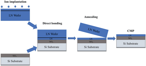
Deposition methods such as evaporation, sputtering and chemical vapor deposition could make LN thin film that was polycrystalline in most cases [Citation7–10]. The polycrystalline thin film would cause high optical transmission loss due to the scattering of light at the grain boundary. Single-crystal LN thin film could be physically stripped from the LN bulk material and transferred to the supporting substrate through a series of processes such as ion implantation, direct bonding and thermal annealing [Citation11]. shows the fabrication process of LNOI. First, a layer of SiO2 was grown on an Si substrate by thermal oxidation, and helium (He) ions were implanted into the polishing side of LN wafer. Then, the implanted surface was directly bonded to the SiO2 substrate surface and annealed at high temperature. During the annealing process, the implanted He ions formed bubbles which would connect with each other and split the LN thin film from the LN wafer. Further annealing was used to repair the lattice damage of LN thin film caused by ion implantation. Finally, chemical mechanical polishing (CMP) was used to remove the damaged layer on the surface of the LN thin film and reduce the surface roughness. To support LN thin film, various handles have been developed, such as LN, sapphire, SiC, and quartz. Currently, the maximum size of LNOI wafers is 8 inches [Citation12]. The lapping and polishing method could also produce high-quality LNOIs, which had a smaller influence on crystal quality but put strict requirements on thickness uniformity control [Citation13].
Figure 1. Fabrication process of LNOI.
2.2. Fabrication of passive LNOI devices
The development of nanostructuring techniques has been accompanied by the emerging thin-film LNOI platform [Citation14–16]. In the initial phase of LNOI photonics, weakly confined waveguides have been fabricated on LNOI platform with a small index constrast Δn < 0.1 by metal diffusion, ion exchange, or proton exchange techniques, leading to a limit of integration density and poor performance of device caused by the large bend radius and large mode size [Citation17,Citation18]. Subsequently, high index contrast photonic structures such as waveguides, photonic crystal cavities and whispering gallery microcavities have been successfully produced with controllable manufacture and high anisotropy by dry etching techniques based on physical etching, chemical etching, and the combination of physical and chemical etching. There are some milestones in the high-quality fabrication on LNOI platform.
In 2005, argon ion beam milling was first extended to etch LNOI with the assistant of photoresist (PR) mask defined by lithography, using argon ion plasma to physically remove the materials [Citation19]. However, the fabricated LNOI structures suffer high scattering loss from the rough sidewall of the structures because of relatively low resolution of the use of standard optical lithography [Citation20,Citation21] and laser lithography [Citation22,Citation23]. The propagation loss was limited to the order of magnitude of 10 dB/cm, and the optical Q factor of the whispering gallery microcavity is only 104 [Citation24]. In 2009, focused ion beam (FIB) milling has been used to fabricate photonic structures on thin-film LN with high flexibility [Citation25,Citation26]. It is suitable to fabricate cliff-sidewall structures like photonic crystal cavity. However, to make a tradeoff between the low fabrication efficiency and fabrication resolution, the fabricated waveguides possess rough surface because of the re-deposition of etched material caused by the large beam-current FIB. Therefore, the propagation loss of the LNOI structures was much high because of the rough sidewall, which limits the potential photonic applications.
In 2014, a modified FIB milling method, which employed femtosecond laser ablation to etch LNOI into semifinished microstructures to improve the fabrication efficiency, and then used two-step FIB milling to polish the sidewall with high resolution and suppress the re-deposition, was developed to fabricate high-quality photonic structures in LNOI [Citation27,Citation28]. The reported loaded Q factors reached 2.5 × 10⁵ at that time and have been improved to close to 107 now by employing lower beam current of several hundred pA at voltage of 30 kV in the secondary milling to minimize surface re-deposition of the removed LN [Citation29,Citation30]. About five months later, electron-beam lithography (EBL) assisted argon ion milling was developed with high resolution to fabricate low-loss photonic structures [Citation31]. The pattern of the photonic structure was defined in hydrogen silsesquioxane (HSQ) resist with multipass exposure by standard EBL with ~125 keV, and transferred to thin-film LN by argon ion milling to physically bombard and etch the exposed LN material. The loaded Q factors of the fabricated microcavities reached 1.02 × 10⁵ at that time by argon ion etching at a bias voltage of ~180 V and an RF power of 200W with an etch rate of ~30 nm/min and a selectivity of ~ 1:1 using a reactive ion etching tool. And the best loaded Q factors have been improved to up to 5.0 × 10⁶ [Citation32], by argon ion milling using a commercial inductively coupled plasma reactive ion etching (ICP RIE) tool with optimal plasma power and chamber condition to minimize surface re-deposition of removed LN and other contaminations present in the chamber, and coating a cladding SiO2 layer to suppress the scattering loss, corresponding to an ultra-low propagation loss of 2.7 dB/m in the telecom band. Besides FIB milling and coating with a cladding layer, chemo-mechanical polishing has been also used to polish the side wall of the fabricated LNOI structures [Citation33], and the loaded Q factor was further improved to close to 107 [Citation34]. And the wedge angle of the fabricated side wall is 60 ~ 70ο by argon ion milling, and 80ο by FIB milling. However, the writing field (typically smaller than 1 mm2), the fabrication cost, and the fabrication efficiency are still limited by the use of FIB and EBL.
In 2018, femtosecond laser photo-lithography assisted chemo-mechanical etching (PLACE) was developed to fabricate ultra-low loss LNOI structures, allowing wafer-scale manufacturing with high speed [Citation35–37]. To fabricate ultra-low loss structures, a chromium hard mask was prepared on LNOI wafer by femtosecond laser ablation with a speed up to 2 m/s and a relatively high resolution of 200 nm [Citation38]. Then the pattern of the structure was transferred from the hard mask to the LNOI layer by etching the exposed thin-film LN through chemo-mechanical polishing. After removing the hard mask, secondary chemo-mechanical polishing was carried out to further produce an ultra-smooth surface with average roughness reaches 0.1 nm. Since this technique is an ion-free processing, ultra-low loss structures with an ultra-high intrinsic Q factor up to 108 and a low propagation loss of 0.34 dB/m in 1550 nm waveband were achieved on LNOI platform [Citation39,Citation40], avoiding inner lattice damage of LN which was traditionally introduced by ion slicing and ion milling. Moreover, the writing field of the femtosecond laser photo-lithography is only limited by the displacement stage, which can be longer than 20 cm, wafer-scale integration up to 8-inch can be achieved by PLACE. shows the ultra-high Q microdisk with intrinsic Q factor of 1.23 × 10⁸ in 1550 nm wave band. Monolithic microring side-coupled with waveguides [Citation41] fabricated by PLACE is plotted in . And an array of 1960 Mach-Zehnder interferometer (MZI) structures fabricated on a 4-inch wafer [Citation38] was plotted in . The total lithography time for patterning the MZI array is only 2.3 hrs, which exhibits that each MZI of 10 mm total length can be patterned within only 4.3 second, which is suitable for industrial-scale mass-production. The deficiency of PLACE technique is difficulty in the fabrication of cliffy side-wall structure with wedge angle > 50ο, such as photonic crystal cavities.
Figure 2. (a) The ring-down measurement of the ultra-high Q microcavity [Citation39], exhibiting an intrinsic Q factor of 1.23 × 10⁸. Inset: the scanning electron microscope (SEM) image of the microdisk, where the scale bar is 200 μm. (b) SEM image of the monolithic microring [Citation41]. (c) Photograph of an array of 1960 MZIs patterned in a 4-inch wafer. (d) Micrograph of unbalanced MZI. Inset: zoom-in micrographs of 1×2 multi-mode interferometer (MMI) and Euler bend waveguide [Citation38].
![Figure 2. (a) The ring-down measurement of the ultra-high Q microcavity [Citation39], exhibiting an intrinsic Q factor of 1.23 × 10⁸. Inset: the scanning electron microscope (SEM) image of the microdisk, where the scale bar is 200 μm. (b) SEM image of the monolithic microring [Citation41]. (c) Photograph of an array of 1960 MZIs patterned in a 4-inch wafer. (d) Micrograph of unbalanced MZI. Inset: zoom-in micrographs of 1×2 multi-mode interferometer (MMI) and Euler bend waveguide [Citation38].](/cms/asset/545c91e2-529d-4a92-a4f8-03d8e7acfbf0/tapx_a_2322739_f0002_oc.jpg)
For mass production with low cost, ultraviolet (UV) lithography assisted argon ion milling was first proposed to fabricate high-quality photonic structures on LNOI platform in 2015 [Citation42]. Here, a premanufactured mask is must for expose the photoresist to pattern the microstructures [Citation42,Citation43]. And the loaded Q factors of the microcavities over 106 were first demonstrated on LNOI platform at that time [Citation42]. Recently, deep ultraviolet (DUV) lithography which allows a smaller line-edge-roughness of the waveguide followed by argon ion milling has been used to fabricate photonic devices with wafer scale. 6-inch wafer scale fabrication has been demonstrated with a propagation loss of 0.27 dB/cm [Citation44]. More recently, 8-inch wafer scale thin-film LN has been used to produced photonic devices with propagation loss of 0.47 ± 0.09 dB/cm using 193 ArF lithography [Citation45], as shown in . To further reduce the propagation loss, the PR should be reflowed with high temperature annealing at temperatures greatly exceeding its glass transition temperature to reduce sidewall surface roughness [Citation47] to sub-nm root mean square roughness, and the fabricated devices should be annealing with high temperature to restore the lattice damage caused by ion implantation and ion milling [Citation16,Citation21,Citation28,Citation48].
Figure 3. (a) Photography of 8-inch wafer during DUV lithography. (b) Optical micrograph of a spiral LNOI waveguide with a length of 11.49 cm [Citation45]. (c) The illustration of the fabrication of thin-film PPLN waveguide [Citation46]. (d) The optical micrograph of the waveguides and periodic poled domains [Citation43].
![Figure 3. (a) Photography of 8-inch wafer during DUV lithography. (b) Optical micrograph of a spiral LNOI waveguide with a length of 11.49 cm [Citation45]. (c) The illustration of the fabrication of thin-film PPLN waveguide [Citation46]. (d) The optical micrograph of the waveguides and periodic poled domains [Citation43].](/cms/asset/de61352a-492f-4eb8-b349-1fdd7e93b9c1/tapx_a_2322739_f0003_oc.jpg)
Wet etching has also been developed to fabricate photonic structures with high Q factors by etching the -Z face [Citation49–51]. This technique suffers anisotropy etching, and is not favored for some applications, for example, high-speed electro-optic modulation in X-cut wafer, and periodically poled lithium niobate (PPLN) nonlinear optics. The comparison of the aforementioned fabrication methods is shown in .
Table.1. Comparison of different fabrication methods in terms of the-state-of-the-art propagation losses, loaded Q factors, minimum feature sizes, and integration scales, available by each method.
An alternative scheme to utilize the outstanding optical properties of LNOI is loading strip waveguides with a similar refractive index material such as silicon nitride for defining waveguides by the deposition and etching of the strip material [Citation53–61], or a low refractive index organic polymer by patterning using photonic bound states in the continuum (BIC) [Citation62–64] on LNOI. This technique often called etch-less technique or strip loading of thin-film LN. Multiplexer, polarization convertor, spectrometer, nonlinear optical convertor, and electro-optic modulator have been demonstrated on such hybrid platform [Citation53]. The advancement of etch-less technique has been well summarized in Ref [Citation53]. We will give a brief overview on this technique. There are several advantages in this fabrication method. First, we get rid of the difficulty in the etching of LNOI, and are benefitted from the mature fabrication of the loading materials. Second, we can employ various material platforms such as silicon, silicon nitride, polymer, Chalcogenide materials integrated with LNOI thin-film to form photonic chip with multi-functionalities, by taking full advantage of these materials and the high nonlinearity and large electro-optic coefficient of LN. However, a fraction of the optical modal power is leaked to reside in the strip material which lowers optical conversion efficiencies in processes that benefit from the optical nonlinearity of LN.
And for nonlinear optical applications and quantum light sources, thin-film periodically poled lithium niobate (PPLN) waveguides and microcavities have shown greater potentials than bulk counterpart to access the highest optical coefficient d33, in terms of compact structures, low power consumption, and high modulation. High-quality poling process has been demonstrated in-situ on thin-film LNOI by applying strong electric field using some tools, including microelectrodes structure [Citation65,Citation66] patterned on the LNOI wafer defined by lift-off electron-beam lithography [Citation46,Citation67,Citation68] (as shown in , and atomic force microscopy/piezoelectric force microscopy (AFM/PFM) tip [Citation69,Citation70] with high manufacturing resolution. Here, the poling structure patterned by microelectrodes often needs coercive field ≥ 20 kV/mm. For the electrodes defined by electron-beam lithography, poling often requires voltage pulses with amplitude up to 600 V depending on the distance between the electrodes and pulse width of sub-second, and is suitable for both X-cut and Z-cut LNOI wafer. Meanwhile, the poling based on microelectrodes can be performed before or after the nanostructuring of LNOI structures. While for AFM/PFM-tip poling, since the AFM machine can not provide voltage pulse with high amplitude (typically less than 200 V), a metal layer is needed to be placed underneath the thin film LN with a smaller minimum poling period down to 400 nm [Citation70]. Therefore, AFM/PFM-tip poling is suitable for partially free-standing microstructure where the bottom metal layer can be undercut to reduce the loss, and it is difficult to be extended to unsuspended waveguides. Besides in-situ poling, poling pattern can be done in the bulk crystal, and then transferred to thin-film wafer using ion-slicing, and finally was nanostructuring for waveguide fabrication [Citation43], as shown in .
2.3. Fabrication of active LNOI devices
To form a PIC, active photonic devices, such as microlasers, detectors, modulators, optical amplifers are indispensable. For modulators, high speed electro-optic Mach-Zenhder modulators with bandwidth exceeding 100 GHz has been demonstrated both by etching LN and strip loading, integrated with microelectrodes fabricated by traditional metal lift-off process or femtosecond laser ablation.
For microlasers, thin-film LN does not provide optical gain for lasing, akin to silicon. One strategy to obtain optical gain is to embed gain medium such as rare earth ions in thin-film LN by ion implantation into the thin film or directly growth of the doped crystal during crystal growth and then ion slicing [Citation71–74], as shown in . Although ion implantation can be carried out locally with space selectivity followed by certain annealing process to activate the doped ions for quantum memories [Citation76], which is favored for multi-functional photonic integration, the uniformity of doped ion and the ion activity are poorer for lasing than that of the latter method. And the implantation concentration is still relatively low for providing enough optical gain for lasing. The doping via crystal growth method is uniformity with ions populated in the entire thin-film LN wafer.
Figure 4. (a) Illustration of the growth of erbium ion doped bulk LN crystal [Citation74]. (b) Schematic of the fabrication of passive and active LNOI photonics by stitching and nanostructuring [Citation75].
![Figure 4. (a) Illustration of the growth of erbium ion doped bulk LN crystal [Citation74]. (b) Schematic of the fabrication of passive and active LNOI photonics by stitching and nanostructuring [Citation75].](/cms/asset/eb5c5e5b-2185-441d-9b11-fa6d8beafab3/tapx_a_2322739_f0004_oc.jpg)
Rare-earth ions, such as erbium ion and ytterbium ion, have been doped solely or co-doped in bulk LN for providing optical gain around 1530 nm and 1030 nm wavelength, respectively. Then the doped bulk LN is sliced to thin-film LNOI by ion-slicing and bonding. Subsequently, photonic structures such as whispering gallery microcavities, Fabry-Perot resonator based on Sagnac loop reflectors, and waveguides fabricated on the active thin-film LN by PLACE and dry etching techniques. However, since the thin-film LN is entirely doped, it is unfavourable for integrating with other passive photonic devices on single chips. Therefore, a monolithically integrated active and passive waveguide array has been demonstrated by stitching the active wafer with passive wafer tightly together for nanostructuring [Citation75], as shown in .
The other strategy is integration of the passive thin-film LN photonic devices with electrically pumped microlasers based on III-V family gain media [Citation77]. The III-V laser diodes are fabricated on chips. Then the light sources are coupled into the undoped LNOI devices through transfer printing, hybrid integration, flip-chip bonding, and heterogeneous integration, providing on-chip light sources in the C-band using electrical drivers [Citation78–81]. And distributed feedback (DFB) laser chips have been employed to pump the miniature ultrafast laser source [Citation82] and integrated optical isolator [Citation83] on LNOI wafer using this strategy.
The third strategy is to optically align and package high-gain chips such as III-V gain sections and LNOI chips consisting of passive-cavities like loop mirrors together, by mimicking the integrated external-cavity-diode-laser-structures in silicon photonics [Citation84,Citation85]. The outstanding advantage of this strategy is fast laser frequency tuning and electro-optical reconfigurability enabled by LNOI with mW-scale outpower power. Integrated Pockels laser with high-speed modulation and second harmonic generation [Citation84] has been demonstrated.
Because LNOI is an electrical insulator and does not possess a PN-junction, optical detectors should be incorporated using integrated photodiodes based on semiconductor materials like silicon and III-V materials, or pyroelectric effect of LN [Citation86–90]. Heterogeneous integration of amorphous silicon [Citation91] photodetector was first demonstrated on LNOI waveguides operating in the visible wavelength range with responsivity ≤37 mA/W, by leveraging the transition between the conduction band (CB) and valence band. Then III – V photodiodes [Citation79,Citation92,Citation93] have also been heterogeneously integrated on LNOI waveguides operating in the 1550 nm band, featuring a wide bandwidth of 80 GHz and a responsivity of 0.6 A/W. Superconducting nanowire single photon detectors [Citation94–97], have been integrated on LNOI ridge waveguides using niobium nitride (NbN) nanowires and niobium titanium nitride (NbTiN) nanowires, offering high detection efficiency up to 46% [Citation96], low dark count rates as low as 13 Hz, and short timing jitters as low as 17 ps at cryogenic temperature [Citation97]. Black phosphorus photoconductors [Citation98,Citation99], 2D graphene photodetectors [Citation88], hetero-integrated MoS2-based self-powered photodetectors [Citation100], have also been demonstrated on LNOI platform with high performance, thanks to the outstanding properties of 2D materials exploiting the broad bandwidth, the tunable bandgap structures and high carrier mobility [Citation101]. For example, a 2D graphene p-n junction photodetector reported on LN by Guan et al. shows a wide detection ranging from 405 to 2000 nm, a high responsivity of 2.92 × 10⁶ A/W, and a detectivity of 8.65 × 10¹⁴ Jones. Another kind of photodetectors has proposed by implementing silver nanoparticles into LNOI platform [Citation89] operating with a broadband from 520 nm to 1900 nm by enhancing photovoltaic effect, showing a high responsivity of 0.25 A/W, fast response time of 16 ms, and good photocurrent stability with instability below 0.3%). Large bandwidth, small dark account, small timing jitter, durability and high detection sensitivity are required for improve the performance of the devices. Furthermore, to directly form p-n junction in LNOI platform, electric-field poling has been used to fabricate n-type and p-type conductive domain walls for forming of ferroelectric-domain-wall p-n junction in LNOI platform [Citation102], exhibiting a high electron and hole mobilities in the corresponding domain walls of 337 and 93 cm2 V−1 s−1, respectively.
3. Application of LNOI devices
LNOI is an outstanding PIC platform candidate. Taking advantage of the strong mode confinement in LNOI circuit, the nonlinear-optical, electro-optical and acousto-optic performance of LN is greatly enhanced to one of the highest level among all platforms. Leveraging such high coefficients, high-efficient nonlinear parametric process, high-speed and flexible on-chip optical manipulation can be achieved, resulting in breakthrough in modulators, frequency converters, optical frequency combs, quantum optical circuits and integrated lasers, as discussed below.
3.1. Modulators
Traditional electro-optic (EO) LN modulators have gained widespread popularity in long-haul communication systems. However, traditional EO LN modulators, based on ion-diffused or proton-exchange optical waveguides on bulk LN crystals [Citation17], suffer from weak confinement, requiring the placement of electrodes far away from the waveguides to minimize the metal absorption losses. Consequently, modulation efficiency is low (typically >10 V·cm), necessitating long modulation regions (at least 10 cm) to achieve sub-1 V Vπ (half-wave voltage). The high RF loss from the long electrodes also limits the electro-optic bandwidth to approximately 35 GHz.
The LNOI platform has revolutionized LN modulator performance by addressing these limitations. One key advancement is the success of the fabrication for highly confined waveguides in LNOI, allowing small-gapped electrodes without additional metal absorption losses. This significantly enhances the interaction between electric and optical fields compared to traditional LN modulators [Citation103–109]. Patterned LNOI waveguides have been successfully implemented to achieve low-loss, high-speed, and energy-efficient travelling-wave LN modulators. Alternative waveguide formation methods include rib-loaded waveguides [Citation60,Citation110,Citation111], SOI-bonded [Citation112], and SiNx-bonded waveguides [Citation113]. However, these approaches have limited mode confinement factors (<81%), resulting in moderate modulation efficiency compared to the dry-etched LNOI modulators. Besides, the exploration of thermo-optic (TO) TFLN modulators has been somewhat limited due to their slow response time in the order of tens of microseconds. However, the thermo-optic effect is preferred for stably operating EO modulators at the desired operational conditions to ensure optimal performance [Citation114].
Figure 5. (a) LNOI modulator with regular coplanar waveguides, with a Vπ of 1.4V and an EO bandwidth of 45 GHz [Citation103]. (b) Advanced LN IQ modulators [Citation104]. (c) Integrated LNOI modulators with capacity-loaded travelling electrodes and quartz substrate [Citation105].
![Figure 5. (a) LNOI modulator with regular coplanar waveguides, with a Vπ of 1.4V and an EO bandwidth of 45 GHz [Citation103]. (b) Advanced LN IQ modulators [Citation104]. (c) Integrated LNOI modulators with capacity-loaded travelling electrodes and quartz substrate [Citation105].](/cms/asset/37887ec5-05dd-4163-9687-4cd63ddcc512/tapx_a_2322739_f0005_oc.jpg)
Significant progress has been made in increasing the bandwidth of LNOI-based modulators [Citation115]. Notable achievements include an integrated LN Mach-Zehnder modulator with regular coplanar waveguides, with a Vπ of 1.4 V and an EO bandwidth of 45 GHz [Citation103], as shown in . Advanced LN IQ modulators have been demonstrated with drive voltages of 1.9 V and 3.1 V, EO bandwidths exceeding 48 GHz and 67 GHz, and impressive modulation capabilities for various advanced modulator formats [Citation104], as shown in . More importantly, integrated LNOI modulators with capacity-loaded travelling electrodes and a quartz substrate have greatly improved the voltage-bandwidth performance, resulting in low RF loss (0.21 dB/cm/GHz1/2), a flat EO response, and Vπ of 1.3 V with a 20-mm-long modulator [Citation105], as shown in .
In the field of intensity-modulated direct-detection (IM-DD) modulation, an integrated LNOI Mach-Zehnder modulator (MZM) achieved an exceptional line rate of 700 Gb/s [Citation109]. Moving on to dual-polarization coherent systems, a remarkable net data rate of 1.58 Tb/s per wavelength was accomplished using a 200 Gbaud probabilistically shaped 64-QAM signal, by employing a LNOI IQ modulator and a discrete polarization-division multiplexing (PDM) emulator [Citation108]. Furthermore, a recent advancement involved a LNOI dual-polarization in-phase quadrature (DP-IQ) modulator integrated with an on-chip polarization rotator and combiner (PRC) [Citation116]. This device utilized optimized 23.5-mm-long CL-TWEs to achieve low half-wave voltage of 1 V and a large EO bandwidth of 110 GHz, as shown in . Such a high-performance DP-IQ modulator achieved a record-breaking net bitrate of up to 1.96 Tb/s and demonstrated ultra-low power consumption (1.04 fJ/bit) using a 130 Gbaud probabilistic constellation shaping (PCS-) 400QAM scheme. More recently, a DP-IQ modulator featuring a record symbol-rate of 220 GBaud modulation rate was also demonstrated, showing great promise for next generation optical communications [Citation117].
Figure 6. (a) LNOI dual-polarization in-phase quadrature (DP-IQ) modulator integrated with an on-chip polarization rotator and combiner (PRC) [Citation116]. (b) Modulator with folded MZMs incorporating meander traveling wave electrode and optical waveguides [Citation118]. (c) Wafer-scale low-loss lithium niobate photonic integrated circuits [Citation44].
![Figure 6. (a) LNOI dual-polarization in-phase quadrature (DP-IQ) modulator integrated with an on-chip polarization rotator and combiner (PRC) [Citation116]. (b) Modulator with folded MZMs incorporating meander traveling wave electrode and optical waveguides [Citation118]. (c) Wafer-scale low-loss lithium niobate photonic integrated circuits [Citation44].](/cms/asset/b4c84409-f022-49fd-8707-7d76d390a700/tapx_a_2322739_f0006_oc.jpg)
Maybe the only one drawback is that LNOI EO modulators require a long phase modulation length of >1 cm to achieve a CMOS-level driving voltage (<1 V). Such devices pose practical difficulties for integration into compact transceiver packages. To address this issue, folded MZMs (as shown in ) incorporating meander traveling wave electrode and optical waveguides have proven effective in reducing the device length while preserving overall performance [Citation118,Citation119]. An alternative way to achieve a compact device size is to use micro-resonator structures [Citation120].
In addition to the advancements in EO modulators, TFLN modulators based on acousto-optic (AO) properties also have demonstrated significantly improved performances compared to those demonstrated on bulk LN, due to stronger confinement for both the acoustic and optical modes, along with enhanced AO interactions. High-performance AO modulators require large mode overlap, long interaction length, and high-power robustness at the same time, achieved by judiciously engineering the configurations of the optical and acoustic components and the relative position between them to achieve low-loss waveguides and high-efficiency interdigital transducers (IDTs).
A method utilizing an IDT to drive a freestanding 100 μm-long thin-film acoustic resonator for modulating light in a Mach – Zehnder interferometer or racetrack cavity has been demonstrated, achieving half-wave voltages of 4.6 V and 0.77 V, respectively [Citation121]. The strong microwave-to-acoustic coupling offered by the transducer in conjunction with the strong photo-elastic, piezoelectric, and electro-optic effects of lithium niobate. In the above case, acoustic waves propagate across an optical waveguide perpendicularly, where the interaction length is insufficient generally, while the collinear and copropagating configuration features a higher electromechanical Brillouin scattering (EBS) efficiency. The suspended one-dimensional (1D) strip AO waveguides with an effective length of 250 μm, has been experimentally demonstrated to achieve a record-setting 18% conversion efficiency corresponding to 30 µW in the SH0 acoustic waves mode and a 3 dB bandwidth of 40 nm, which is inherently nonreciprocal and can be integrated with an optical filter to be a non-magnetic isolator [Citation122].
Additionally, to avoid the etching process of suspended LN waveguides, LN AO modulators with unsuspended waveguides have been reported on LN-on-silicon [Citation123], LN-on-sapphire [Citation124], and LN-on-chalcogenide glasses (ChGs) [Citation125] platforms. A built-in push-pull AO modulation configuration based on the antisymmetric surface acoustic waves (SAW) mode has been experimentally demonstrated to relax the fabrication complexities and double the modulation efficiency compared with the single arm by using the bidirectional acoustic energy in principle, achieving a half-wave voltage as low as 0.03 V cm in the TFLN-ChG hybrid platform [Citation125].
LNOI modulators stand out for its exceptional performance in terms of ultra-low loss, high bandwidth, low Vπ. More importantly, LNOI modulators is on the rise in the commercial market, and the demonstration of wafer-level LN photonics integrated circuits (as shown in ) holds promise for low-cost fabrication [Citation44].
3.2. Nonlinear optical devices
Nonlinear optical effects with high efficiency and low pump power, such as harmonic generation, sum-frequency generation, and parametric processes, have applications in optical communication [Citation126], quantum and nonlinear light sources [Citation127], wavelength converter [Citation128] and so on. LN has excellent nonlinear properties (d33=-27 pm/V), making it a fascinating platform for nonlinear optics with low pump power. Compared with the traditional devices fabricated by proton and titanium diffusion processes, LNOI prepared by the smart-cut process has higher refractive index contrast, especially, by combining the semiconductor fabrication processes, small mode volume, and high integration can be simultaneously obtained. Importantly, the propagation loss of the LN optical waveguide can be reduced to 0.027 dB/cm [Citation32,Citation36]. Based on the good spatial localization and low propagation loss of LNOI photonic devices, it has good prospects in nonlinear optical applications with low pumping, high efficiency, high gain, and low loss. Here, the recent advances of second-order nonlinear optical effect on LNOI photonic devices are reviewed, including new processes and new mechanisms, especially focusing on the functional devices based on second harmonic generation (SHG). Finally, the progresses have been made and the challenges are summarized.
For efficient harmonic generation, usually, the nonlinear phase matching mechanism can be divided into mode phase matching (MPM) and quasi-phase matching (QPM). MPM mechanism always has a request of combination dispersion engineering and modes selection, including quantum number, polarization and even propagation direction relative to the crystal axis. Compared with MPM, QPM is a flexible scheme by designing the poling period and the domain pattern, making full use of nonlinear coefficient of LN, and ensure sufficient mode overlap factor simultaneously. Theoretically, when ignoring the loss of the waveguides, the conversion efficiency of the SHG can be 100%, and the normalized conversion efficiency can be close to 5000% W−1cm−2 in peridically poled LNOI waveguides. The great progress has been made for nonlinear frequency conversion in LN waveguide and resonator, such as the normalized conversion efficiency in PPLN waveguide of 4600% W−1cm−2 [Citation129] and absolute conversion efficiency of 80% [Citation130] in PPLN has been achieved, and the SHG with ultra-high conversion efficiency of 5,000,000% W−1 was obtained in PPLN microcavity [Citation131]. In addition to the nonlinearities associated with QPM, processes of MPM-based nonlinearities were made. Recently, the improvement of the mode overlap factor between the modes involved in nonlinear process by using the different crystal orientation of the dual-layer LN thin film was reported. The efficient SHG based on MPM condition could be achieved by optimizing the structure parameters, such as the thickness of LN thin film and width of the waveguide, the theoretical normalized conversion efficiency calculated to be 10,000% W−1cm-2 [Citation132], and the conversion efficiency of 5540% W−1cm−2 was obtained in experiment [Citation133], as shown in .
Figure 7. MPM second harmonic generation. (a) the two MPM points at 1379.4 nm and 1381.5 nm, the inset figures are the electric profiles of the SH modes [Citation132] (b) the theoretical NCE values versus the relative thicknesses of LN layer [Citation132]. (c) the sketch of ridge waveguide in double-layer LNOI with reversed polarization [Citation133]. (d) Measured SHG spectrum of dual-layer ridge waveguide at room temperature, the inset figure shows the SHG power as a function of the pump power [Citation133].
![Figure 7. MPM second harmonic generation. (a) the two MPM points at 1379.4 nm and 1381.5 nm, the inset figures are the electric profiles of the SH modes [Citation132] (b) the theoretical NCE values versus the relative thicknesses of LN layer [Citation132]. (c) the sketch of ridge waveguide in double-layer LNOI with reversed polarization [Citation133]. (d) Measured SHG spectrum of dual-layer ridge waveguide at room temperature, the inset figure shows the SHG power as a function of the pump power [Citation133].](/cms/asset/f0f8a94a-6dc7-4529-affe-47a16c253187/tapx_a_2322739_f0007_oc.jpg)
Broadband harmonics have applications in production of pulse light sources and broadening of optical frequency comb and so on. It is often necessary to design photonics devices in combination with dispersion engineering and polarization technology. Such as SHG with a 3-dB bandwidth >110 nm in PPLN waveguide [Citation134], as shown in , and broadband SHG in step-chirped PPLN waveguides with a bandwidth of 110 nm [Citation138], as shown in , has been achieved. Recently, instead of the fabrication of the domain structures, the generation of broadband second harmonics based on MPM was realized through the change of waveguide temperature gradient, and the bandwidth is measured to be 15 nm [Citation135]. Besides, tunable light sources are important components of photonic integrated optics. The thermal and electro-optical properties of LN provide effective ways for tunable nonlinear light sources. As an example of the tunable light sources, the SHG signals based on the thermal-optical effect of LN microdisk resonators was reported, and the tuning rate is measured to be 1.68 nm/K [Citation136], as shown in . Furthermore, tunable self-injection locked frequency conversion laser has been reported recently [Citation137], as shown in .
Figure 8. Broadband SHG signals and tunable SHG laser. (a) Measured (black) and theoretical (blue) SHG transfer function for nanophotonic PPLN waveguide, broader than the bulk PPLN (orange) waveguide [Citation134]. (b) Measured broadening of birefringence phase matching spectra at different temperature gradients [Citation135]. (c-d) temperature sensitive SHG laser [Citation136,Citation137].
![Figure 8. Broadband SHG signals and tunable SHG laser. (a) Measured (black) and theoretical (blue) SHG transfer function for nanophotonic PPLN waveguide, broader than the bulk PPLN (orange) waveguide [Citation134]. (b) Measured broadening of birefringence phase matching spectra at different temperature gradients [Citation135]. (c-d) temperature sensitive SHG laser [Citation136,Citation137].](/cms/asset/2d8481fc-052f-46cc-b8cb-5eee45270121/tapx_a_2322739_f0008_oc.jpg)
For other nonlinear effects and applications. Recently, sum-frequency generation in high Q x-cut thin film LN microdisk via cyclic QPM were reported, and the conversion efficiency was measured to be 2.52 × 10⁻⁴ mW−1 [Citation139]. In addition, the quantum frequency conversion from infrared to visible band by sum-frequency generation was achieved, and the single photon detection with efficiency measured to be 8.7% [Citation140]. In addition to focusing the light field interaction in the cavity, the second harmonic radiation field was detected in the LN microring resonator, and the mechanism of nonlinear optical radiation and the coupling with free space were further investigated [Citation141]. It is not limited by the resonant state of the signal light in the microcavity, and can be applied in the detection of the SHG spectrum.
In conclusion, LNOI has both second-order nonlinear properties of monocrystalline materials and higher optical integration, providing fascinating platform for related all optical nonlinear. Up to date, various nonlinear optical devices have already been demonstrated basing on both X- and Z-cut peridically poled LNOI waveguide. Detailed SHG conversion efficiencies are summarized in . However, various applications still suffer from challenges, and can be further investigated. (1) In terms of nonlinear conversion efficiency, there is still a lot of room for improvement, and the conversion efficiency is affected by multiple indicators of the device, such as multi-frequency resonant or not in the microcavity system, and whether the phase matching conditions are satisfied and so on. (2) The reduction of propagation loss including the bending loss and the scattering loss, and the insert loss, such as the coupling between the waveguide and the fiber lens and waveguide-cavity coupling will benefit the nonlinear conversion of efficiency. (3) The device interconnection and light field control, including the combination of thermal-optical, electro-optical effects and nonlinear frequency conversion, such as the tuning range, accuracy and stability and so on.
Table 2. Comparison of SHG conversion efficiencies in peridically poled LNOI waveguide devices.
3.3. Optical frequency combs
Owing to the χ(3) nonlinearities of lithium niobate, Kerr optical frequency comb based on four-wave mixing can be realized in LNOI. Kerr frequency combs are the most common form of frequency combs used in LNOI and other material platforms. Wang et al. first demonstrated wide-spanning Kerr comb generation in LNOI (~300 nm for TM modes and ~700 nm for TE modes) [Citation151]. He et al. showed the self-starts and bi-directional switching of soliton states in Z-cut LNOI due to the photorefractive effect. Second-harmonic combs and Raman-induced soliton frequency shift were also discussed [Citation152]. They also demonstrated perfect soliton crystal in a Z-cut LNOI, which could realize the comb line spacing from 1 to 11 times of the free-spectral range of the resonator by adjusting the pump power and wavelength () [Citation153]. Perfect soliton crystal expands the application scenarios of LNOI, but still needs a smaller FSR to be used in communications. Gong et al showed the soliton microcomb around 2 um [Citation157] and demonstrated the soliton microcombs spectral span up to 4/5 octaves in LNOI by careful dispersion engineering () [Citation154]. Lately, Wan et al. demonstrated a stable soliton by the photorefractive effect of LNOI and demonstrated turnkey soliton generation () [Citation158]. Cheng et al. pump the microcavity using a tunable on-chip femtosecond pulse to expand the Kerr frequency comb span. The output frequency comb spans 400 nm in bandwidth and consists of over 1400 comb lines with a pump-to-comb conversion efficiency of 10% [Citation156]. Lithium niobate has a mature rare earth ion doping technology; researchers also carried out optical comb exploration in rare earth ion doped LNOI. Yang et al. realized a single soliton in Yb-doped Z-cut LNOI, which has a spectrum span around 180 nm [Citation155].
Figure 9. Kerr frequency combs based on LNOI (a) soliton crystals with different soliton numbers [Citation153]. (b) single-soliton and wo-soliton microcombs with near-octave soliton bandwidth [Citation154]. (c) (d) the soliton spectrum and step in a ytterbium-doped lithium-niobate microring [Citation155]. (e) Measurement scheme and optical spectrum of pulse-pumped Kerr frequency combs [Citation156].
![Figure 9. Kerr frequency combs based on LNOI (a) soliton crystals with different soliton numbers [Citation153]. (b) single-soliton and wo-soliton microcombs with near-octave soliton bandwidth [Citation154]. (c) (d) the soliton spectrum and step in a ytterbium-doped lithium-niobate microring [Citation155]. (e) Measurement scheme and optical spectrum of pulse-pumped Kerr frequency combs [Citation156].](/cms/asset/3ebf2360-3f59-456d-96b4-c5970ad50185/tapx_a_2322739_f0009_oc.jpg)
Besides, the high χ(2) nonlinearities and the limitation of light of LNOI make it possible to realize the electro-optic (EO) modulator with high bandwidth and low power consumption [Citation103,Citation159,Citation160], so as to realize the EO frequency comb with high performance. Optical frequency combs generated based on χ(2) nonlinearity, in other words, the EO frequency comb, can be briefly divided into two categories: resonant devices and non-resonant devices. As for resonant devices, the Ground-Signal-Ground electrodes should place along the straight section of a high-Q microcavity, and the modulation frequency should match the FSR of the resonator for wide-range combs generation. Zhang et al. first demonstrated the EO frequency comb based on a racetrack microring resonator on LNOI with a frequency span of about 60 nm [Citation161]. Hu et al. improved the above device by adding a ring resonator coupling with the racetrack resonator [Citation162]. The efficiency was improved from ~ 0.3% to 30% with an optical span of 132 nm (). In terms of application, Shams-Ansari et al. demonstrate the EO microring-based dual-comb interferometer for measuring the absorption and dispersion spectra of gas-phase acetylene() [Citation163]. Javid et al. generated a broadband entangled-photon quantum optical frequency comb using periodic poling technology in a dispersion-engineered X-cut LNOI resonator spanning 30-THz bandwidth and 600 comb lines [Citation166]. The non-resonant EO combs devices are more inclined to use amplitude or phase modulators or cascaded both for a flat-band and low energy-consumption comb generation [Citation82,Citation164,Citation165,Citation167,Citation168]. Renaud et al. realized visible to near-infrared EO combs with low optical loss, high bandwidth, and flat-top spectra by using a Mach-Zehnder modulator () [Citation165]. Zhang et al. demonstrate a power-efficient LNOI-based EO comb with 47 comb lines at a 25-GHz repetition rate () [Citation164]. It is worth noting that they chose a UV Stepper lithography system for sample fabrication, which is advantageous for large-scale integration. Non-resonant EO combs have also been applicated in dual-comb spectroscopy for gas detection [Citation169,Citation170]. Compared with resonant EO combs based on high-Q resonators, non-resonant EO combs tend to more flexible and have a flat spectral. They can arbitrarily adjust the pump wavelength and RF frequency over a large range without the limitation of FSR. However, on the other hand, they often have relatively low bandwidth and fewer comb lines in contrast to resonant EO combs.
Figure 10. (a) EO comb generated by two coupled resonators for effective spectrum broadening [Citation162]. (b) Schematic of dual-comb spectroscopy for gas detection based on racetrack resonator [Citation163]. (c) Structure of power-efficient on-chip EO comb and combs with different pump wavelengths [Citation164]. (d) Structure of Mach-Zehnder modulator for visible-to-near-infrared electro-optic frequency combs [Citation165].
![Figure 10. (a) EO comb generated by two coupled resonators for effective spectrum broadening [Citation162]. (b) Schematic of dual-comb spectroscopy for gas detection based on racetrack resonator [Citation163]. (c) Structure of power-efficient on-chip EO comb and combs with different pump wavelengths [Citation164]. (d) Structure of Mach-Zehnder modulator for visible-to-near-infrared electro-optic frequency combs [Citation165].](/cms/asset/1cb512cc-f52c-4c4f-8cec-6a34aa414d8b/tapx_a_2322739_f0010_oc.jpg)
The researchers tried to take full advantage of the rich optical properties of lithium niobate by combining a variety of nonlinear processes to produce optical frequency combs with higher performance. One of the most notable is the supercontinuum [Citation171–176]. Supercontinuum is generated by using an ultrashort pulse as the pump and subjecting it to various nonlinear effects such as self-phase modulation, stimulated Raman scattering, and optical parametric processes in a highly nonlinear material. This process ultimately leads to the generation of a broad and flat spectrum. Lu et al. demonstrate an octave-spanning supercontinuum generation from 700 nm to 2400 nm in LNOI waveguides with anomalous dispersion using pulsed laser. After that, Jankowski et al. [Citation173] and Yu et al. [Citation174] demonstrated more than two octaves of frequency span supercontinuum in LNOI waveguide using relatively low pulse energy. Okawachi et al. showed f-2f interferometer through second-harmonic generation and subsequent supercontinuum generation in a single dispersion-engineered LN waveguide. These days, Wu et al. achieved supercontinuum from 330 nm to 2400 nm within a pump pulse power as low as 90 pJ in a multi-segment LNOI waveguide which combines both dispersion and quasi-phase matching engineering [Citation176]. The conversion from 1550 nm into the UV greater than 32%. In addition to the supercontinuum, researchers also performed the combination of Kerr combs and electro-optical combs in X-cut [Citation177] and Z-cut [Citation178] lithium niobate, respectively. A tunable optical frequency comb ranging from visible light to near-infrared is produced by using a variety of nonlinear processes in periodically polarized lithium niobate [Citation179].
In conclusion, with the development of lithium niobate process technology, the performance of LNOI optical frequency combs will also continue to improve. There are still some problems worth considering and addressing; we list here for readers to think about: (1) How to reduce pump power while still realizing a soliton? Integrating multiple photonic devices is the inevitable trend of LNOI development, but most of the soliton realization still needs tens to hundreds of milliwatts of on-chip power. Considering edge coupling loss, this is somewhat difficult to integrate with integrated DFB/DBR lasers. (2) The possibility of dark pulse in LNOI microcavity. There have been some works in other material platforms about generating dark pulse Kerr combs, such as SiN [Citation180–182], but these have yet to be reported in LNOI to the best of our knowledge. Dark pulses can be generated in a normal dispersion microcavity, which greatly expands the freedom of optical comb generation. In addition, the dark pulse has high conversion efficiency and spectral flatness, which is a huge advantage for integration and communication fields. (3) Optical frequency combs based on rare earth ions-doped LNOI. LNOI has relatively mature rare earth ion doping technology. We have reported the production of a single soliton in a Yb-doped LNOI [Citation155], but we think that this is far from taking full effect of rare earth ion-doped LNOI. How to use the luminescence characteristics of rare earth ions to produce high-efficiency and wide-band combs is an urgent problem to be solved. (4) How to fully utilize the mature periodic poling technique in LNOI to generate visible light combs and solitons through frequency doubling/tripling. To sum up, high integration, high efficiency, and wide bandwidth is the future development trend of lithium niobate optical frequency comb, and it is also the direction of our efforts. Taking full advantage of the characteristics of LNOI that are different from other material platforms is the key to improving performance. We look forward to seeing LNOI optical frequency combs used in various fields such as ranging, astronomy, and communications in the future.
3.4. Quantum optical circuit
Quantum integration can support large-scale photonic circuit, with low-loss and phase-sensitive optical path as the interaction, which is essential for realizing complex quantum optics research and quantum information application in small cost [Citation183]. LN-based quantum chip is one of the most promising integrated platform, where diffused LN waveguides have already been widely used for high-quality photon pair generation, single photon frequency conversion and dynamic electro-optical control of phase and frequency for the past decade [Citation184]. Using ultra-strong confined LNOI waveguide, not only the above prevalent devices are lifted to a new record performance, several other essential quantum devices, including on-chip quantum memories and single-photon detectors are also developed by means of doping or heterogeneous integration, towards full-functional integrated quantum chips.
High rate, bright and pure photon pair generation is the fundamental basis of quantum tasks. PPLNOI devices can support efficient and flexible spontaneous parametric down-conversion (SPDC) process and fulfill the requirement. In 2020, Zhao et al first report a high-rate photon-pair source in a straight PPLNOI waveguide under low pump power, reaching a record performance of coincidences-to-accidentals counts ratio (CAR >67000), two-photon interference visibility (V > 99%) and heralded single-photon autocorrelation (g(2) <0.025) simultaneously [Citation185]. In the same year, cavity enhanced SPDC is realized by a micro-ring resonator on PPLNOI, with radius of only 55 μm, reaching a record generation-rate of 2.7 × 10⁹ Hz/mW across all material platforms then [Citation186], as shown in . In 2021, Xue et al report a broadband source with a record generation rate of 2.79 × 10¹¹ Hz/mW and engineered it for eight-channel multiplexed energy-time entanglement with Franson interferences up to 99.17% visibility [Citation187]. By dispersion engineering, ultrabroadband entangled photons generation is also realized on a straight PPLNOI waveguide with 100 THz bandwidth [Citation188]. The ultra-high nonlinearity in LNOI also has the potential for enabling breakthrough in the strong photon-photon interaction, for scalable multi-photon state generation and deterministic photonic logic control between photons, as proposed in a recent theoretical work, as shown in . To make it happen, PPLNOI micoring resonators with 107 is required, which is within the loss limit of LNOI waveguide [Citation189]. Though it is still challenging from the fabrication point of view, once realized, it can greatly push forward the practical application of quantum optical technologies.
Fast, low-loss and dynamic manipulation of large-scale quantum states is essential for complex quantum applications. Utilizing LN-based EOM and AOM, the phase, polarization and frequency freedom of photon state can be manipulated directly on chip, which has already been demonstrated by diffused LN waveguide and widely used in various applications. The highly integrable LNOI devices provides further ability for large-scale quantum circuit. In a most recent work, a LNOI-based integrated optical circuit, including beam splitters and EOMs are used as a quantum processor for fast and reprogrammable universal interferometer for up to two path-coded qubits, showing flexibility and scalability of on-chip quantum state manipulation on LNOI chips [Citation190], as shown in . More particularly, LNOI devices also enable frequency-domain manipulation, and have the ability to unlock infinite-dimensional frequency resources. On-chip electro-optic frequency shifters and frequency domain beam splitters have already been realized by two coupled ring-resonators on a LNOI chip [Citation191], as shown in . Recently, on-chip manipulation of single photon in frequency domain is demonstrated by LNOI-based modulators, reaching a record-high frequency shifting (±641 GHz) and bandwidth compression/expansion [Citation192], paving the way of fully-integrated frequency-coded quantum chips.
Figure 11. (a) High-rate quantum source realized by cavity enhanced SPDC on a micro-ring resonator [Citation186]. (b) Deterministic multi-photon generation scheme [Citation189]. (c) Integrated optical circuit for optical path coded photon state manipulation [Citation190]. (d) Integrated electro-optical frequency splitter for frequency domain manipulation [Citation191].
![Figure 11. (a) High-rate quantum source realized by cavity enhanced SPDC on a micro-ring resonator [Citation186]. (b) Deterministic multi-photon generation scheme [Citation189]. (c) Integrated optical circuit for optical path coded photon state manipulation [Citation190]. (d) Integrated electro-optical frequency splitter for frequency domain manipulation [Citation191].](/cms/asset/407befcf-8172-4e65-b4c2-71fc23a5134c/tapx_a_2322739_f0011_oc.jpg)
Aiming at full-integrated quantum chips, on-chip detection and storage of quantum states are of great significance for quantum computation and communication applications, where several breakthroughs are made on LNOI platform in the past two or three years, as shown in . In terms of single photon detector (SPD), upconversion SPD is mature and most comprehensive at room temperature, a LNOI-based low-noise upconversion SPD is realized using straight PPLNOI waveguide and off-chip silicon single-photon avalanche photodiode (SPAD) this year, achieving an internal conversion efficiency of 73% and detection efficiency of 8.7% [Citation140]. Though limited by optical loss and end-coupling efficiency, a big gap exists between experimental performance of LNOI based and diffused LN based SPD now, where the highest detection efficiency of about 40% is holded [Citation193]. The LNOI waveguide can provide stronger nonlinear interaction with small footprint, enabling breakthroughs of deterministic single photon upconversion under ultra low pump power. On a broader scale, using superconducting nanowire single-photon detectors (SNSPD) instead of upconversion assisted SPAD may lead to significant breakthroughs, which have better performance and can be monolithically integrated in LNOI chips. A NiN SNSPD on LNOI is first reported in 2020, achieving detection efficiency of 46% [Citation96]. Then simultaneous realization of high speed modulation and high efficient detection is achieved at cryogenic temperature by monolithically integrated of SNSPDs and EOMs in a reconfifigurable LNOI waveguide [Citation97]. The above works open a new way for integrated single photon detection, though challenges still exist for adaptability of cryogenic temperature for quantum sources and manipulation. While for storage applications, a so-called single photon buffer is reported by electro-optical controllable loops on LNOI platform this year, achieving up to 1.4 ns storage time with 100 ps steps [Citation194]. For long-term storage, a LNOI-based quantum memory is also realized by Tm3+ doping, with bandwidth of more than 100 MHz and storage time of up to 250 ns [Citation195]. Furthermore, by heterogeneous integration of quantum emitters directly onto the LNOI waveguides with a pick-and-place technique that has recently emerged [Citation196], the key blocks for constructing integrated LNOI quantum chips are already built, paving a potential path of full-functional integrated quantum chips.
Figure 12. (a) LNOI-based superconducting nanowire single-photon detector [Citation97]. (b) LNOI-based low-noise upconversion SPD with off-chip silicon single-photon avalanche photodiode (SPAD) [Citation140]. (c) LNOI-based single photon buffer [Citation194]. (d) LNOI-based quantum memory [Citation195].
![Figure 12. (a) LNOI-based superconducting nanowire single-photon detector [Citation97]. (b) LNOI-based low-noise upconversion SPD with off-chip silicon single-photon avalanche photodiode (SPAD) [Citation140]. (c) LNOI-based single photon buffer [Citation194]. (d) LNOI-based quantum memory [Citation195].](/cms/asset/550b858e-d501-45f9-a553-fc1b1baec378/tapx_a_2322739_f0012_oc.jpg)
LNOI-based quantum devices have achieved highest performance in photon-pair generation, electro-optical photon state manipulation among all integrated platforms, made breakthroughs in untraditional features like quantum storage and SPD, and displayed incomparable advantages in realizing complex quantum sources and full-integrated frequency manipulation. Though the device performance is still limited by current fabrication technologies, full-functional quantum chips can be expected in the future.
3.5. Lasers and amplifiers
Microlasers have been demonstrated on both the active and passive thin-film LN platforms, using optical pump sources and electrical injection, respectively. For rare-earth doped thin-film LN, microlasers were first achieved at 1550 nm wavelength with multi-mode lasing in Er3+ microcavities by three independent groups [Citation71,Citation72,Citation197] and then single-mode microlasers were operated in coupled microcavities using Vernier effect [Citation198–201], as shown in . Single mode microlasers have also been demonstrated in single microrings from fundamental modes and weakly perturbed microdisks from polygon modes. For the former one, single-frequency lasing is often achieved at 1530 nm by employing mode-dependent loss and gain filtering [Citation204,Citation205], since the optical gain is maximum at this wavelength. For the latter one, the single-frequency microlaser was demonstrated around 1550 nm wavelength through the formation of coherently combined polygon modes in the circular microdisks at both pump and laser wavelengths, which are formed by exciting polygon modes via coupling the microdisk with a tapered fiber for introducing weak perturbation. Since the spatial intensity overlap between both polygon modes at pump and laser wavelengths [Citation202] is much higher than that between the polygon pump mode and the traditional whispering gallery lasing mode, all other whispering gallery modes are suppressed, leading to single-frequency lasing. The ultra-high Q factors (>107) of both the pump and lasing polygon modes ensure an ultra-narrow laser fundamental linewidth of ~454 Hz and a low threshold of 25 μW.
The above-mentioned part is focused on the resonant microstructures. The combination of the resonant structures and the choice of doped ions brings in microlasers operated at different waveband, different gain, and threshold. For example, erbium (Er) ions and ytterbium (Yb) ions [Citation206,Citation207] provide coherent light generation at 1550 nm waveband and 1030 nm waveband, respectively. To increase the output power and reduce the threshold, Er and Yb ions co-doping is favored by using Yb ions as sensitized co-dopant ions, because the concentration quenching of Er ions is reduced through energy transfer and the pumping efficiency of the 980-nm band is improved, yielding a more significant gain. Microlaser with threshold less than 1 μW [Citation208,Citation209] has been demonstrated on co-doping platform. And the maximum output power of single-mode microlasers reaches 62 μW, which is mainly limited by the tradeoff between the cavity length and single mode operation [Citation210].
Figure 13. Single-frequency microlasers. (a) Coupled microrings [Citation199]. (b) Coupled microcavities consisted of a microdisk and a microring [Citation201]. (c) Single weakly perturbed microdisk laser from polygon modes [Citation202]. (d) Photograph of long-cavity length coupled microrings [Citation200]. (e) Optical graph of up-conversion fluorescence from Fabry-Perot resonator based on Sagnac loop reflectors [Citation203].
![Figure 13. Single-frequency microlasers. (a) Coupled microrings [Citation199]. (b) Coupled microcavities consisted of a microdisk and a microring [Citation201]. (c) Single weakly perturbed microdisk laser from polygon modes [Citation202]. (d) Photograph of long-cavity length coupled microrings [Citation200]. (e) Optical graph of up-conversion fluorescence from Fabry-Perot resonator based on Sagnac loop reflectors [Citation203].](/cms/asset/edfde1b5-41a0-4a79-a644-689414e665d7/tapx_a_2322739_f0013_oc.jpg)
Besides active whispering gallery microcavities, single-mode microlaser has also been demonstrated on Fabry-Perot resonator based on Sagnac loop reflectors. The output power of microlaser reached 44.7 μW, enabled by the large cavity length of ~4 mm [Citation203]. An electro-optic tuning of the lasing wavelength was achieved with efficiency as high as 1.75 pm/V by applying direct-current bias on the microelectrodes integrated on the cavity waveguide.
The rare-earth doped thin-film LN is also an excellent platform for optical waveguide amplifiers. The waveguide amplifiers were first demonstrated on air-cladding waveguides with a small-signal net gain up to 18 dB [Citation74,Citation211–214]. To further improve the net gain, a cladded waveguide amplifier was demonstrated with large modal area with part of the optical power leaked to the cladding layer for reducing the quenching ions, a net gain more than 20 dB was reported [Citation215]. More recently, a small-signal internal net gain of 27 dB was achieved in the Er-Yb co-doped waveguide amplifier, benefiting from Yb-sensitized-Er in promoting the gain performance and the large mode size for higher gain [Citation216].
In addition to optically pumped microlasers based on rare earth ion doping, electrically pumped microlasers based on III-V or II-VI materials have been integrated on LNOI platforms via transfer printing, hybrid integration, flip-chip bonding, heterogeneous integration [Citation73], since these gain media are favored due to their convenient operation and high gain performance as well as facilitating dense integration. First, Kuyken’s group heterogeneously integrated III-V materials on the thin film LN platform using microtransfer-printed technology and designed the primary devices of amplifiers, multimode microring lasers, and single-mode tunable lasers [Citation81]. Subsequently, Cai’s group reported a widely tunable O-band hybrid LN/III-V laser through butting coupling an InP-based reflective semiconductor optical amplifier (RSOA) to a passive LNOI coupled microring chip [Citation217] integrated with microheaters to thermally adjust the lasing wavelength. Experimentally, the hybrid laser achieved single-mode laser operation with a maximum output power of 2.5 mW by using the vernier effect, and a broadband tuning range of 36 nm was obtained through thermal tuning. Not long after, the Loncar’s group at Harvard University demonstrated a fully integrated high-power laser on the LNOI platform by Ref [Citation78]. A powerful DFB laser was integrated into a pre-etched trench of the passive LNOI chip front-end using a flip-chip process, achieving on-chip power of up to 60 mW. At the same time, the researcher also built a high-power transmitter by combining the laser with a LNOI electro-optic modulator, obtaining a 3 dB bandwidth of 50 GHz. Thanks to the integration of lasers, this high-power transmitter is expected to improve the stability and scalability of data center interconnection, as well as reduce the cost of the entire system. Otherwise, Cai’s group also reported an O-band transmitter with by hybrid integrated an III-V reflective semiconductor optical amplifier (RSOA) chip to a passive LNOI Mach – Zehnder modulator. In addition, lasers based on heterogeneously integrated III – V-on-LNOI also be demonstrated recently by the same group [Citation79,Citation218]. Another kind of hybrid microlasers has also demonstrated by butt-coupling an electrically pumped microlaser chip with active LNOI microresonators. Here, the 980-nm electrically pumped lasers only serve as on-chip pump light source to excite the on-chip 1550-nm microlasers [Citation219], showing a narrower linewidth of 0.05 nm by leveraging the high-Q LNOI active microresonator.
On the other hand, in addition to basic elements such as power and linewidth, the fast adjustability and reconfigurability of lasers are also considered important functions, such as LiDAR requiring lasers to have a linear modulation rate of MHz level with GHz-level chirping range. To this end, Lin’s group based on the integrated III-V/LNOI external-cavity-diode-laser structure, demonstrated a record-high frequency modulation speed of laser using the Pockels effect of LN [Citation84]. The configuration diagram of the entire integrated Pockels laser is shown in , RSOA and passive LNOI chip are integrated through butting coupling. In the LNOI external cavity structure, besides the loop mirror, two racetrack microrings is designed to achieve single-mode lasing based on the Vernier effect. Moreover, micro heater, driving electrodes as well as PPLN section are incorporated to enrich the functionality of the laser. In the experiment, stable linear adjustment was achieved across a broad range frequency up to 600 MHz by applying a driving electrical signal to the phase shifter, reaching a modulation speed of 2.0 × 10¹⁸ Hz/s, as shown in . In addition, the fast on-off switching of lasing mode with a switching speed of 50 MHz and the high-speed synchronous modulation of a two-color laser () is also achieved in this system. Compared to the common thermal wavelength tuning on silicon or silicon nitride platforms, this integrated Pockels laser significantly improves the frequency-modulation rate and reduces power consumption. In addition, a self-injection locked frequency conversion laser at visible waveband is also reported from Lin’s group based a similar integration scheme, achieving a on-chip power of 2 mW and 4.7 kHz linewidth [Citation137]. Around the same time, Kippenberg’s group at EPFL also reported an ultrafast tunable laser using LN integrated photonics [Citation220]. The laser consists of a hybrid integration of an InP DFB laser diode and an external resonator chip, and the self-injection locking can be initiated by butt-coupling as shown in . The sectional diagram of the external chip is shown in . To obtain the narrow linewidth and frequency-agile tuning of the laser, the external resonator is manufactured on the Si3N4 photonic integration platform by the Damascene process with ultralow loss and then bonding a layer of thin film Lithium niobate for fast tuning. In the experiment, the laser operated with an intrinsic linewidth of 3.14 kHz and a frequency tuning speed of 12 × 1015 Hz/s is demonstrated with a drive voltage of 25 Vpp. Further demonstrating the low noise and fast tuning ability of the laser, researchers also performed an optical ranging experiment using the confirmed laser, achieving a resolution of about 15 cm in a lab environment. depicted the point cloud image of three-dimensional optical ranging. Subsequently, to reduce the drive voltage of the laser fast tuning, the research group developed a tightly bound LN photonic chip as an external cavity chip to enhance the electro-optical interaction and achieved a frequency modulation speed of 0.7 × 10¹² Hz/s under a CMOS-compatible drive voltage (2 Vpp) [Citation80]. Recently, an LNOI external-cavity-diode-structure microlaser has recently reported by inserting an integrated RSOA chip between a fiber Bragg grating and a tunable LNOI Sagnac loop reflector (TSLR), showing an output power of 738.8 μW, an intrinsic linewidth of 45.55 kHz, and an electro-optical frequency tuning range of 20 GHz at the C band [Citation85].
Figure 14. (a) Schematic illustration of the integrated pockels laser [Citation84]. (b) Recorded laser frequency modulation rate for the increasing modulation speed [Citation84]. (c) Optical spectra of the dual-color lasing based on the SHG process [Citation84]. (d) Integrated schematic diagram of the ultrafast tunable laser [Citation220]. (e) False-colour SEM image of waveguide cross-section for a heterogeneously integrated Si3N4-LiNbO3 external cavity chip [Citation220]. (f) Point-cloud of the measured target scene in the three-dimensional optical ranging experiment [Citation220].
![Figure 14. (a) Schematic illustration of the integrated pockels laser [Citation84]. (b) Recorded laser frequency modulation rate for the increasing modulation speed [Citation84]. (c) Optical spectra of the dual-color lasing based on the SHG process [Citation84]. (d) Integrated schematic diagram of the ultrafast tunable laser [Citation220]. (e) False-colour SEM image of waveguide cross-section for a heterogeneously integrated Si3N4-LiNbO3 external cavity chip [Citation220]. (f) Point-cloud of the measured target scene in the three-dimensional optical ranging experiment [Citation220].](/cms/asset/67057adb-31ba-4c48-9ad1-b69ccf3d6b88/tapx_a_2322739_f0014_oc.jpg)
To summarize this part, the optical-pump active LNOI microlaser possess superiority in narrow fundamental linewidth, the ease to fabrication, and the choices of operation waveband depending on the doped ions. And the maximum output power of the microlaser is limited to several tens of microwatt due to the limited optical gain provided by the limited doped concentration for maintaining the crystal quality and the tradeoff between cavity length and single mode operation. Whilst, the output power of the electrical injection LNOI light sources provide much higher power >60 mW. The linewidth of the such lasers is on the order of magnitude of sub-MHz. To achieve microlasers with higher performance, high output power, fast switching, narrow linewidth of sub-kHz, and electrical injection are highly in demand, which can compromise the merits of the two styles [Citation219].
Besides above applications that we discuss, LN-based metasurfaces design has potential application in the fields of nonlinear optics, LiDAR, AR/VR and quantum photonics [Citation221–223], and has been demonstrated for efficient second harmonic generation [Citation224,Citation225], waveguide mode conversion [Citation226], and on-chip optical manipulation [Citation227–229].
4. Conclusion
Within a short period of merely one decade, thin film LN photonics has witnessed a remarkable progress enabling a plurality of photonic devices featuring unprecedented performance. Single-crystal LN thin film on various substrates have been produced by the smart cut with wafer size up to 8 inch and several high-quality fabrication techniques have been developed. The fabrication approach chosen by most research groups is electron beam lithography combined with ionic dry etch, resulting in high fabrication resolution and smooth sidewall in the fabricated structures such as waveguides and microdisk resonators. Alternatively, ultraviolet (UV) and deep UV (DUV) lithography has also been employed for mask patterning, which offers much higher fabrication efficiency than the EBL lithography while the fabrication resolution is significantly poorer. Besides the etching approaches, another fabrication technology called PLACE has been developed, which is interesting for its potential to produce stitching-less integrated photonic circuits, with large-footprint and low propogation loss simultaenously.
The obvious and unique advantages of thin film LN is its large electro-optic coefficient and second-order nonlinear effect. In addition, the high Curie temperature of LN allows it to survive from the semiconductor processing which is also critical for photonic integration application. LNOI modulators have reached low energy consumption and high tuning rate, which is the key to achieve ultra-high speed information processing towards information infrastructure. Nonlinear devices with high conversion efficiency, broad bandwidth and flexible tunability have been developed for optical frequency conversion. Basing on these, on-chip Kerr and EO frequency combs are developed with higher integration, efficiency, and wider bandwidth, which may be used in ranging, astronomy and communications. In quantum optics, the LNOI devices push the photon-pair generation efficiency and photon state manipulation flexibility to a new level, supporting full-functional quantum optical circuits with high-rate quantum sources and full-integrated frequency-coded state manipulators, and the potential of deterministic photon-photon interaction is also revealed. Besides, high performance optical-pump and electrical injection active microlasers and amplifiers have also been developed on LNOI.
These techniques have produced a broad spectrum of integrated photonic devices and systems as discussed above which are mostly demonstrated with innovative functionalities and outstanding performance in the laboratories worldwide. The main obstacles for these devices to enter the commercial market are the production cost and reproducibility, which will be the focus of the future investigations for many research groups actively working in this area today.
Acknowledgments
The authors thank Tao Li, Qiang Luo, Heyun Tan, Zhenzhong Hao, Renhong Gao, Shuting Kang, Qingyun Li for their assistance in editing text, figures and references.
Disclosure statement
No potential conflict of interest was reported by the authors.
Additional information
Funding
References
- Sun J, Hao Y, Zhang L, et al. Brief review of Lithium Niobate crystal and its applications. J Synth Cryst. 2020;49:947–964.
- Gao B, Ren M, Zheng D, et al. Long-lived Lithium Niobate: history and progress. J Synth Cryst. 2021;50:1183–1199.
- Boes A, Chang L, Langrock C, et al. Lithium niobate photonics: unlocking the electromagnetic spectrum. Science. 2023;379:eabj4396. doi: 10.1126/science.abj4396
- Vazimali MG, Fathpour S. Applications of thin-film lithium niobate in nonlinear integrated photonics. Adv Photon. 2022;4:034001. doi: 10.1117/1.AP.4.3.034001
- Xie R-R, Li G-Q, Chen F, et al. Microresonators in lithium niobate thin films. Adv Opt Mater. 2021;9:2100539. doi: 10.1002/adom.202100539
- https://seas.harvard.edu/news/2017/12/now-entering-lithium-niobate-valley.
- Nakata Y, Gunji S, Okada T, et al. Fabrication of LiNbO3 thin films by pulsed laser deposition and investigation of nonlinear properties. Appl Phys A. 2004;79:1279–1282. doi: 10.1007/s00339-004-2748-1
- Yoon J-G, Kim K. Growth of highly textured LiNbO3 thin film on si with MgO buffer layer through the sol-gel process. Appl Phys Lett. 1996;68:2523–2525. doi: 10.1063/1.115842
- Lansiaux X, Dogheche E, Remiens D, et al. LiNbO3 thick films grown on sapphire by using a multistep sputtering process. J Appl Phys. 2001;90:5274–5277. doi: 10.1063/1.1378332
- Sakashita Y, Segawa H. Preparation and characterization of LiNbO3 thin films produced by chemical-vapor deposition. J Appl Phys. 1995;77:5995–5999. doi: 10.1063/1.359183
- Poberaj G, Hu H, Sohler W, et al. Lithium niobate on insulator (LNOI) for micro-photonic devices. Laser Photonics Rev. 2012;6:488–503. doi: 10.1002/lpor.201100035
- Ren M, Xu J, Lan P, et al. Roadmap on nonlinear optics–focus on Chinese research. J Phys Photonics. 2023;5:032501. doi: 10.1088/2515-7647/acdb17
- Li Q, Zhang H, Zhu H, et al. Characterizations of single-crystal lithium niobate thin films. Crystals. 2022;12:667. doi: 10.3390/cryst12050667
- Szafraniak I, Radu I, Scholz R, et al. Single-crystalline ferroelectric thin films by ion implantation and direct wafer bonding. Integr Ferroelectr. 2003;55:983–990. doi: 10.1080/10584580390259452
- Solal M, Pastureaud T, Ballandras S, et al. Oriented lithium niobate layers transferred on 4” (100) silicon wafer for RF SAW devices. IEEE International Ultrasonic Symposium. Munich, Germany; 2002. p. 131–134.
- Rabiei P, Gunter P. Optical and electro-optical properties of submicrometer lithium niobate slab waveguides prepared by crystal ion slicing and wafer bonding. Appl Phys Lett. 2004;85:4603–4605. doi: 10.1063/1.1819527
- Wooten EL, Kissa KM, Yi-Yan A, et al. A review of lithium niobate modulators for fiber-optic communications systems. IEEE J Sel Top Quant. 2000;6:69–82. doi: 10.1109/2944.826874
- Parameswaran KR, Route R, Kurz JR, et al. Highly efficient second-harmonic generation in buried waveguides formed by annealed and reverse proton exchange in periodically poled lithium niobate. Opt Lett. 2002;27:179–181. doi: 10.1364/OL.27.000179
- Rabiei P, Steier WH. Lithium niobate ridge waveguides and modulators fabricated using smart guide. Appl Phys Lett. 2005;86:161115. doi: 10.1063/1.1906311
- Guarino A, Poberaj G, Rezzonico D, et al. Electro–optically tunable microring resonators in lithium niobate. Nat Photonics. 2007;1:407–410. doi: 10.1038/nphoton.2007.93
- Hu H, Ricken R, Sohler W. Lithium niobate photonic wires. Opt Express. 2009;17:24261–24268. doi: 10.1364/OE.17.024261
- Poberaj G, Koechlin M, Sulser F, et al. Ion-sliced lithium niobate thin films for active photonic devices. Opt Mater. 2009;31:1054–1058. doi: 10.1016/j.optmat.2007.12.019
- Koechlin M, Poberaj G, Günter P. High-resolution laser lithography system based on two-dimensional acousto-optic deflection. Rev Sci Instrum. 2009;80:085105. doi: 10.1063/1.3202274
- Poberaj G, Koechlin M, Sulser F, et al. High-density integrated optics in ion-sliced lithium niobate thin films. Conference on Integrated Optics: Devices, Materials, and Technologies XIV. San Francisco, CA; 2010. p. 76040U.
- Sulser F, Poberaj G, Koechlin M, et al. Photonic crystal structures in ion-sliced lithium niobate thin films. Opt Express. 2009;17:20291–20300. doi: 10.1364/OE.17.020291
- Hu H, Yang J, Gui L, et al. Lithium niobate-on-insulator (LNOI): status and perspectives. Conference on Silicon Photonics and Photonic Integrated Circuits III. Brussels, Belgium; 2012. p. 84311D.
- Lin J, Xu Y, Fang Z, et al. Second harmonic generation in a high-Q lithium niobate microresonator fabricated by femtosecond laser micromachining. arXiv. 2014;1405:6473.
- Lin J, Xu Y, Fang Z, et al. Fabrication of high-Q lithium niobate microresonators using femtosecond laser micromachining. Sci Rep. 2015;5:8072. doi: 10.1038/srep08072
- Lin J, Yao N, Hao Z, et al. Broadband quasi-phase-matched harmonic generation in an on-chip monocrystalline lithium niobate microdisk resonator. Phys Rev Lett. 2019;122:173903. doi: 10.1103/PhysRevLett.122.173903
- Ge L, Jiang H, Liu Y, et al. Quality improvement and mode evolution of high-Q lithium niobate micro-disk induced by “light annealing”. Opt Mater Express. 2019;9:1632–1639. doi: 10.1364/OME.9.001632
- Wang C, Burek M, Lin Z, et al. Integrated high quality factor lithium niobate microdisk resonators. Opt Express. 2014;22:30924–30933. doi: 10.1364/OE.22.030924
- Zhang M, Wang C, Cheng R, et al. Monolithic ultra-high-Q lithium niobate microring resonator. Optica. 2017;4:1536–1537. doi: 10.1364/OPTICA.4.001536
- Wolf R, Breunig I, Zappe H, et al. Cascaded second-order optical nonlinearities in on-chip micro rings. Opt Express. 2017;25:29927–29933. doi: 10.1364/OE.25.029927
- Wolf R, Breunig I, Zappe H, et al. Scattering-loss reduction of ridge waveguides by sidewall polishing. Opt Express. 2018;26:19815–19820. doi: 10.1364/OE.26.019815
- Wu R, Zhang J, Yao N, et al. Lithium niobate micro-disk resonators of quality factors above 107. Opt Lett. 2018;43:4116–4119. doi: 10.1364/OL.43.004116
- Wu R, Wang M, Xu J, et al. Long low-loss-lithium niobate on insulator waveguides with sub-nanometer surface roughness. Nanomaterials. 2018;8:910. doi: 10.3390/nano8110910
- Zhou J, Gao R, Lin J, et al. Electro-optically switchable optical true delay lines of meter-scale lengths fabricated on lithium niobate on insulator using photolithography assisted chemo-mechanical etching. Chin Phys Lett. 2020;37:084201. doi: 10.1088/0256-307X/37/8/084201
- Chen J, Liu Z, Song L, et al. Ultra-high-speed high-resolution laser lithography for lithium niobate integrated photonics. Frontiers in Ultrafast Optics: Biomedical, Scientific, and Industrial Applications XXII. San Francisco, CA; 2023.
- Gao R, Zhang H, Bo F, et al. Broadband highly efficient nonlinear optical processes in on-chip integrated lithium niobate microdisk resonators of Q-factor above 108. New J Phys. 2021;23:123027. doi: 10.1088/1367-2630/ac3d52
- Gao R, Yao N, Guan J, et al. Lithium niobate microring with ultra-high Q factor above 108. Chin Opt Lett. 2022;20:011902. doi: 10.3788/COL202220.011902
- Li C, Guan J, Lin J, et al. Ultra-high Q lithium niobate microring monolithically fabricated by photolithography assisted chemo-mechanical etching. Opt Express. 2023;31:31556–31562. doi: 10.1364/OE.498086
- Wang J, Bo F, Wan S, et al. High-Q lithium niobate microdisk resonators on a chip for efficient electro-optic modulation. Opt Express. 2015;23:23072–23078. doi: 10.1364/OE.23.023072
- Zhang Y, Li H, Ding T, et al. Scalable, fiber-compatible lithium-niobate-on-insulator micro-waveguides for efficient nonlinear photonics. Optica. 2023;10:688–693. doi: 10.1364/OPTICA.489383
- Luke K, Kharel P, Reimer C, et al. Wafer-scale low-loss lithium niobate photonic integrated circuits. Opt Express. 2020;28:24452–24458. doi: 10.1364/OE.401959
- Wang HY, Xu Y, Li ZY, et al. Thin-film lithium niobate photonic devices on 8-inch silicon substrates. Optical Fiber Communications Conference and Exhibition (OFC). San Diego, CA; 2023.
- Niu Y, Lin C, Liu X, et al. Optimizing the efficiency of a periodically poled LNOI waveguide using in situ monitoring of the ferroelectric domains. Appl Phys Lett. 2020;116:101104. doi: 10.1063/1.5142750
- Prabhakar K, Reano R. Fabrication of low loss lithium niobate rib waveguides through photoresist reflow. IEEE Photon J. 2022;14:1–8. doi: 10.1109/JPHOT.2022.3222184
- Shams-Ansari A, Huang G, He L, et al. Reduced material loss in thin-film lithium niobate waveguides. APL Photon. 2022;7:081301. doi: 10.1063/5.0095146
- Hu H, Ricken R, Sohler W, et al. Lithium niobate ridge waveguides fabricated by Wet Etching. IEEE Photonics Technol Lett. 2007;19:417–419. doi: 10.1109/LPT.2007.892886
- Yang F, Fang X, Chen X, et al. Monolithic thin film lithium niobate electro-optic modulator with over 110 GHz bandwidth. Chin Opt Lett. 2022;20:022502. doi: 10.3788/COL202220.022502
- Zhuang R, He J, Qi Y, et al. High- Q thin-film lithium niobate microrings fabricated with Wet Etching. Adv Mater. 2023;35:2208113. doi: 10.1002/adma.202208113
- Wang L, Clube F, Dais C, et al. Sub-wavelength printing in the deep ultra-violet region using displacement Talbot Lithography. Microelectron Eng. 2016;161:104–108. doi: 10.1016/j.mee.2016.04.017
- Chen G, Li N, Ng JD, et al. Advances in lithium niobate photonics: development status and perspectives. Adv Photon. 2022;4:034003. doi: 10.1117/1.AP.4.3.034003
- Rabiei P, Ma J, Khan S, et al. Heterogeneous lithium niobate photonics on silicon substrates. Opt Express. 2013;21:25573–25581. doi: 10.1364/OE.21.025573
- Chang L, Li Y, Volet N, et al. Thin film wavelength converters for photonic integrated circuits. Optica. 2016;3:531–535. doi: 10.1364/OPTICA.3.000531
- Solmaz M, Adams D, Tan W, et al. Vertically integrated As2S3 ring resonator on LiNbO3. Opt Lett. 2009;34:1735–1737. doi: 10.1364/OL.34.001735
- Cao L, Aboketaf A, Wang Z, et al. Hybrid amorphous silicon (a-Si: H)–LiNbO3 electro-optic modulator. Opt Commun. 2014;330:40–44. doi: 10.1016/j.optcom.2014.05.021
- Bo F, Wang J, Cui J, et al. Lithium‐niobate–Silica hybrid Whispering‐Gallery‐mode resonators. Adv Mater. 2015;27:8075–8081. doi: 10.1002/adma.201504722
- Li S, Cai L, Wang Y, et al. Waveguides consisting of single-crystal lithium niobate thin film and oxidized titanium stripe. Opt Express. 2015;23:24212–24219. doi: 10.1364/OE.23.024212
- Rao A, Patil A, Rabiei P, et al. High-performance and linear thin-film lithium niobate mach–zehnder modulators on silicon up to 50 GHz. Opt Lett. 2016;41:5700–5703. doi: 10.1364/OL.41.005700
- Han X, Jiang Y, Frigg A, et al. Mode and polarization‐division multiplexing based on silicon nitride loaded lithium niobate on insulator platform. Laser Photonics Rev. 2022;16:2100529. doi: 10.1002/lpor.202100529
- Yu Z, Tong Y, Tsang H, et al. High-dimensional communication on etchless lithium niobate platform with photonic bound states in the continuum. Nat Commun. 2020;11:2602. doi: 10.1038/s41467-020-15358-x
- Yu Z, Xi X, Ma J, et al. Photonic integrated circuits with bound states in the continuum. Optica. 2019;6:1342–1348. doi: 10.1364/OPTICA.6.001342
- Yu Y, Yu Z, Wang L, et al. Ultralow‐loss Etchless lithium niobate integrated Photonics at Near‐Visible wavelengths. Adv Opt Mater. 2021;9:2100060. doi: 10.1002/adom.202100060
- Hu H, Gui L, Ricken R, et al. Towards nonlinear photonic wires in lithium niobate. In: Integrated optics: devices, materials, and technologies XIV; San Francisco, California, United States; 2010. p. 76040R.
- Mackwitz P, Rüsing M, Berth G, et al. Periodic domain inversion in x-cut single-crystal lithium niobate thin film. Appl Phys Lett. 2016;108:152902. doi: 10.1063/1.4946010
- Wang C, Langrock C, Marandi A, et al. Ultrahigh-efficiency wavelength conversion in nanophotonic periodically poled lithium niobate waveguides. Optica. 2018;5:1438–1441. doi: 10.1364/OPTICA.5.001438
- Lu J, Surya JB, Liu X, et al. Periodically poled thin-film lithium niobate microring resonators with a second-harmonic generation efficiency of 250,000%/W. Optica. 2019;6:1455–1460. doi: 10.1364/OPTICA.6.001455
- Gainutdinov R, Volk T, Zhang H. Domain formation and polarization reversal under atomic force microscopy-tip voltages in ion-sliced LiNbO3 films on SiO2/LiNbO3 substrates. Appl Phys Lett. 2015;107:162903. doi: 10.1063/1.4934186
- Hao Z, Zhang L, Gao A, et al. Periodically poled lithium niobate whispering gallery mode microcavities on a chip. Sci China Phys Mech Astron. 2018;61:114211. doi: 10.1007/s11433-018-9241-5
- Liu Y, Yan X, Wu J, et al. On-chip erbium-doped lithium niobate microcavity laser. Sci China Phys Mech Astron. 2021;64:234262. doi: 10.1007/s11433-020-1625-9
- Luo Q, Hao Z, Yang C, et al. Microdisk lasers on an erbium-doped lithium-niobite chip. Sci China Phys Mech Astron. 2021;64:234263. doi: 10.1007/s11433-020-1637-8
- Wang M, Fang Z, Lin J, et al. Integrated active lithium niobate photonic devices. Jpn J Appl Phys. 2023;62:SC0801. doi: 10.35848/1347-4065/aca986
- Chen Z, Xu Q, Zhang K, et al. Efficient erbium-doped thin-film lithium niobate waveguide amplifiers. Opt Lett. 2021;46:1161–1164. doi: 10.1364/OL.420250
- Zhou Y, Zhu Y, Fang Z, et al. Monolithically integrated active passive waveguide array fabricated on thin film lithium niobate using a single continuous photolithography process. Laser Photonics Rev. 2023;17:2200686. doi: 10.1002/lpor.202200686
- Wang S, Yang L, Cheng R, et al. Incorporation of erbium ions into thin-film lithium niobate integrated photonics. Appl Phys Lett. 2020;116:151103. doi: 10.1063/1.5142631
- Luo Q, Bo F, Kong Y, et al. Advances in lithium niobate thin-film lasers and amplifiers: a review. Adv Photon. 2023;5:034002. doi: 10.1117/1.AP.5.3.034002
- Shams-Ansari A, Renaud D, Cheng R, et al. Electrically pumped laser transmitter integrated on thin-film lithium niobate. Optica. 2022;9:408–411. doi: 10.1364/OPTICA.448617
- Zhang X, Liu X, Ma R, et al. Heterogeneously integrated III–v-on-lithium niobate broadband light sources and photodetectors. Opt Lett. 2022;47:4564–4567. doi: 10.1364/OL.468008
- Li Z, Wang R, Lihachev G, et al. Tightly confining lithium niobate photonic integrated circuits and lasers. 2022:arXiv:220805556.
- Op de Beeck C, Mayor F, Cuyvers S, et al. III/V-on-lithium niobate amplifiers and lasers. Optica. 2021;8:1288–1289. doi: 10.1364/OPTICA.438620
- Yu M, Barton Iii D, Cheng R, et al. Integrated femtosecond pulse generator on thin-film lithium niobate. Nature. 2022;612:252–258. doi: 10.1038/s41586-022-05345-1
- Yu M, Cheng R, Reimer C, et al. Integrated electro-optic isolator on thin-film lithium niobate. Nat Photonics. 2023;17:666–671. doi: 10.1038/s41566-023-01227-8
- Li M, Chang L, Wu L, et al. Integrated Pockels laser. Nat Commun. 2022;13:5344. doi: 10.1038/s41467-022-33101-6
- Zhu Y, Yu S, Fang Z, et al. Integrated electro-optically tunable narrow-linewidth III-V laser [internet]. arXiv; 2023 [cited 2023 Dec 27]. Available from: http://arxiv.org/abs/2311.15315.
- Suen J, Fan K, Montoya J, et al. Multifunctional metamaterial pyroelectric infrared detectors. Optica. 2017;4:276–279. doi: 10.1364/OPTICA.4.000276
- Gopalan K, Janner D, Nanot S, et al. Mid-infrared pyroresistive graphene detector on LiNbO 3. Adv Opt Mater. 2017;5:1600723. doi: 10.1002/adom.201600723
- Guan H, Hong J, Wang X, et al. Broadband, high‐Sensitivity graphene photodetector based on ferroelectric polarization of lithium niobate. Adv Opt Mater. 2021;9:2100245. doi: 10.1002/adom.202100245
- Sun X, Sheng Y, Gao X, et al. Self-powered lithium niobate thin-film photodetectors. Small. 2022;18:2203532. doi: 10.1002/smll.202203532
- Jin C, Wang C, Qu L, et al. Fast lithium niobate photodetector. Laser Photonics Rev. 2023;17:2300503. doi: 10.1002/lpor.202300503
- Desiatov B, Lončar M. Silicon photodetector for integrated lithium niobate photonics. Appl Phys Lett. 2019;115:121108. doi: 10.1063/1.5118901
- Yi-Yan A, Chan W, Gmitter TJ, et al. Grafted GaAs detectors on lithium niobate and glass optical waveguides. IEEE Photonics Technol Lett. 1989;1:379–380. doi: 10.1109/68.43385
- Guo X, Shao L, He L, et al. High-performance modified uni-traveling carrier photodiode integrated on a thin-film lithium niobate platform. Photonics Res. 2022;10:1338–1343. doi: 10.1364/PRJ.455969
- Colangelo M, Desiatov B, Zhu D, et al. Superconducting nanowire single-photon detector on thin film lithium niobate photonic waveguide. Conference on Lasers and Electro-Optics. San Jose, CA; 2020. p. SM4O.4.
- Höpker JP, Bartnick M, Meyer-Scott E, et al. Towards integrated superconducting detectors on lithium niobate waveguides. Conference on Quantum Photonic Devices. San Diego, California, United States; 2017. p. 1035809.
- Sayem AA, Cheng R, Wang S, et al. Lithium-niobate-on-insulator waveguide-integrated superconducting nanowire single-photon detectors. Appl Phys Lett. 2020;116:151102. doi: 10.1063/1.5142852
- Lomonte E, Wolff MA, Beutel F, et al. Single-photon detection and cryogenic reconfigurability in lithium niobate nanophotonic circuits. Nat Commun. 2021;12:6847. doi: 10.1038/s41467-021-27205-8
- Wang S, Chapman RJ, Johnson BC, et al. Integration of black phosphorus photoconductors with lithium niobate on insulator photonics. Adv Opt Mater. 2023;11:2201688. doi: 10.1002/adom.202201688
- Xue Y, Wu X, Chen K, et al. Waveguide integrated high-speed black phosphorus photodetector on a thin film lithium niobate platform. Opt Mater Express. 2023;13:272–281. doi: 10.1364/OME.477278
- He Z, Guan H, Liang X, et al. Broadband, polarization-sensitive, and self-powered high-performance photodetection of hetero-integrated MoS2 on lithium niobate. Research. 2023;6:0199. doi: 10.34133/research.0199
- Gan X, Shiue R-J, Gao Y, et al. Chip-integrated ultrafast graphene photodetector with high responsivity. Nat Photon. 2013;7:883–887. doi: 10.1038/nphoton.2013.253
- Qian Y, Zhang Y, Xu J, et al. Domain-Wall p - n Junction in Lithium Niobate Thin Film on an Insulator. Phys Rev Appl. 2022;17:044011. doi: 10.1103/PhysRevApplied.17.044011
- Wang C, Zhang M, Chen X, et al. Integrated lithium niobate electro-optic modulators operating at CMOS-compatible voltages. Nature. 2018;562:101–104. doi: 10.1038/s41586-018-0551-y
- Xu M, He M, Zhang H, et al. High-performance coherent optical modulators based on thin-film lithium niobate platform. Nat Commun. 2020;11:3911. doi: 10.1038/s41467-020-17806-0
- Kharel P, Reimer C, Luke K, et al. Breaking voltage–bandwidth limits in integrated lithium niobate modulators using micro-structured electrodes. Optica. 2021;8:357–363. doi: 10.1364/OPTICA.416155
- Wang X, Weigel PO, Zhao J, et al. Achieving beyond-100-GHz large-signal modulation bandwidth in hybrid silicon photonics mach zehnder modulators using thin film lithium niobate. APL Photon. 2019;4:096101. doi: 10.1063/1.5115243
- Yuguang Z, Mengyue X, Hongguang Z, et al. 220 Gbit/s optical PAM4 modulation based on lithium niobate on insulator modulator. 45th European Conference on Optical Communication; Dublin, Ireland. 2019.
- Chen X, Raybon G, Che D, et al. Transmission of 200-GBaud PDM probabilistically shaped 64-QAM signals modulated via a 100-GHz thin-film LiNbO3 I/Q modulator. Optical Fiber Communications Conference and Exhibition (OFC); Washington, DC United States. 2021. p. F3C.5.
- Chen X, Cho J, Raybon G, et al. Single-wavelength and single-Photodiode 700 gb/s entropy-loaded PS-256-QAM and 200-GBaud PS-PAM-16 Transmission over 10-km SMF. 2020 European Conference on Optical Communications (ECOC); Brussels, Belgium. 2020. p. 1–4.
- Chiles J, Fathpour S. Mid-infrared integrated waveguide modulators based on silicon-on-lithium-niobate photonics. Optica. 2014;1:350–355. doi: 10.1364/OPTICA.1.000350
- Rao A, Patil A, Chiles J, et al. Heterogeneous microring and Mach-Zehnder modulators based on lithium niobate and chalcogenide glasses on silicon. Opt Express. 2015;23:22746–22752. doi: 10.1364/OE.23.022746
- Weigel PO, Zhao J, Fang K, et al. Bonded thin film lithium niobate modulator on a silicon photonics platform exceeding 100 GHz 3-dB electrical modulation bandwidth. Opt Express. 2018;26:23728–23739. doi: 10.1364/OE.26.023728
- Boynton N, Cai H, Gehl M, et al. A heterogeneously integrated silicon photonic/lithium niobate travelling wave electro-optic modulator. Opt Express. 2020;28:1868–1884. doi: 10.1364/OE.28.001868
- Wang M, Li J, Yao H, et al. Thin-film lithium-niobate modulator with a combined passive bias and thermo-optic bias. Opt Express. 2022;30:39706–39715. doi: 10.1364/OE.474594
- Xu M, Cai X. Advances in integrated ultra-wideband electro-optic modulators [Invited]. Opt Express. 2022;30:7253–7274. doi: 10.1364/OE.449022
- Xu M, Zhu Y, Pittalà F, et al. Dual-polarization thin-film lithium niobate in-phase quadrature modulators for terabit-per-second transmission. Optica. 2022;9:61. doi: 10.1364/OPTICA.449691
- Mardoyan H, Almonacil S, Jorge F, et al. First 260-GBd single-carrier coherent transmission over 100 km distance based on novel arbitrary waveform generator and thin-film lithium niobate I/Q modulator. In: Leuthold J, and Limberger H, editors 2022 European Conference on Optical Communication (ECOC); Basel Switzerland. Optica Publishing Group; 2022. p.Th3C.2.
- Hu J, Li C, Guo C, et al. Folded thin-film lithium niobate modulator based on a poled mach–zehnder interferometer structure. Opt Lett. 2021;46:2940–2943. doi: 10.1364/OL.426083
- Sun S, Xu M, He M, et al. Folded heterogeneous silicon and lithium niobate Mach–Zehnder modulators with low drive voltage. Micromach. 2021;12:823. doi: 10.3390/mi12070823
- Xue Y, Gan RF, Chen KX, et al. Breaking the bandwidth limit of a high-quality-factor ring modulator based on thin-film lithium niobate. Optica. 2022;9:1131–1137. doi: 10.1364/OPTICA.470596
- Shao L, Yu M, Maity S, et al. Microwave-to-optical conversion using lithium niobate thin-film acoustic resonators. Optica. 2019;6:1498–1505. doi: 10.1364/OPTICA.6.001498
- Sarabalis CJ, Laer RV, Patel RN, et al. Acousto-optic modulation of a wavelength-scale waveguide. Optica. 2021;8:477–483. doi: 10.1364/OPTICA.413401
- Jiang W, Patel RN, Mayor FM, et al. Lithium niobate piezo-optomechanical crystals. Optica. 2019;6:845–853. doi: 10.1364/OPTICA.6.000845
- Sarabalis CJ, McKenna TP, Patel RN, et al. Acousto-optic modulation in lithium niobate on sapphire. APL Photon. 2020;5:086104. doi: 10.1063/5.0012288
- Wan L, Yang Z, Zhou W, et al. Highly efficient acousto-optic modulation using nonsuspended thin-film lithium niobate-chalcogenide hybrid waveguides. Light: Sci Appl. 2022;11:145. doi: 10.1038/s41377-022-00840-6
- Gaur T, Mishra P, Hegde G, et al. Modeling and Analysis of Device Orientation, Analog and Digital Performance of Electrode Design for High Speed Electro-Optic Modulator. Photonics. 2023;10:3.
- Baida FI, Robayo Yepes JJ, Ndao A. Giant second harmonic generation in etch-less lithium niobate thin film. J Appl Phys. 2023;133. doi: 10.1063/5.0142816
- Park T, Stokowski HS, Ansari V, et al. High-efficiency second harmonic generation of blue light on thin-film lithium niobate. Opt Lett. 2022;47:2706. doi: 10.1364/OL.455046
- Rao A, Abdelsalam K, Sjaardema T, et al. Actively-monitored periodic-poling in thin-film lithium niobate photonic waveguides with ultrahigh nonlinear conversion efficiency of 4600 %W −1 cm −2. Opt Express. 2019;27:25920–25930. doi: 10.1364/OE.27.025920
- Chen P-K, Briggs I, Cui C, et al. Adapted poling to break the nonlinear efficiency limit in nanophotonic lithium niobate waveguides. Nat Nanotechnol [Internet]. 2023 [cited 2023 Oct 31]. Available from: https://www.nature.com/articles/s41565-023-01525-w.
- Lu J, Li M, Zou C-L, et al. Toward 1% single-photon anharmonicity with periodically poled lithium niobate microring resonators. Optica. 2020;7:1654. doi: 10.1364/OPTICA.403931
- Du H, Zhang X, Wang L, et al. Highly efficient, modal phase-matched second harmonic generation in a double-layered thin film lithium niobate waveguide. Opt Express. 2023;31:9713–9726. doi: 10.1364/OE.482572
- Wang L, Zhang X, Chen F. Efficient second harmonic generation in a reverse‐polarization dual‐layer crystalline thin film nanophotonic waveguide. Laser Photonics Rev. 2021;15:2100409. doi: 10.1002/lpor.202100409
- Jankowski M, Langrock C, Desiatov B, et al. Ultrabroadband nonlinear optics in nanophotonic periodically poled lithium niobate waveguides. Optica. 2020;7:40–46. doi: 10.1364/OPTICA.7.000040
- Tang Y, Ding T, Lu C, et al. Broadband second-harmonic generation in an angle-cut lithium niobate-on-insulator waveguide by a temperature gradient. Opt Lett. 2023;48:1108–1111. doi: 10.1364/OL.481649
- Yan C, Wang S, Zhao S, et al. Efficient and temperature-tunable second-harmonic generation in a thin film lithium niobate on insulator microdisk. Appl Phys Lett. 2023;122:122. doi: 10.1063/5.0141363
- Ling J, Staffa J, Wang H, et al. Self‐Injection locked frequency conversion laser. Laser Photonics Rev. 2023;17:2200663. doi: 10.1002/lpor.202200663
- Wu X, Zhang L, Hao Z, et al. Broadband second-harmonic generation in step-chirped periodically poled lithium niobate waveguides. Opt Lett. 2022;47:1574–1577. doi: 10.1364/OL.450547
- Zhu J, Sun X, Ding T, et al. Sum-frequency generation in a high-quality thin film lithium niobate microdisk via cyclic quasi-phase matching. J Opt Soc Am B. 2023;40:D44–D49. doi: 10.1364/JOSAB.482270
- Wang X, Jiao X, Wang B, et al. Quantum frequency conversion and single-photon detection with lithium niobate nanophotonic chips. Npj Quantum Inf. 2023;9:1–7. doi: 10.1038/s41534-023-00704-w
- Yang Y, Xu X, Wang J, et al. Nonlinear optical radiation of a lithium niobate microcavity. Phys Rev Appl. 2023;19:034087. doi: 10.1103/PhysRevApplied.19.034087
- Chen J, Sua YM, Ma Z, et al. Efficient parametric frequency conversion in lithium niobate nanophotonic chips. OSA Contin. 2019;2:2914–2924. doi: 10.1364/OSAC.2.002914
- Rao A, Abdelsalam K, Sjaardema T, et al. Actively-monitored periodic-poling in thin-film lithium niobate photonic waveguides with ultrahigh nonlinear conversion efficiency of 4600 %W −1 cm −2. Opt Express. 2019;27:25920–25930. doi: 10.1364/OE.27.025920
- Zhao J, Rüsing M, Javid UA, et al. Shallow-etched thin-film lithium niobate waveguides for highly-efficient second-harmonic generation. Opt Express. 2020;28:19669–19682. doi: 10.1364/OE.395545
- Chen J-Y, Tang C, Ma Z-H, et al. Ultra-efficient and highly-tunable second-harmonic generation in Z-cut periodically poled lithium niobate nanowaveguides. Opt Lett. 2020;45:3789–3792. doi: 10.1364/OL.393445
- Sayem AA, Wang Y, Lu J, et al. Efficient and tunable blue light generation using lithium niobate nonlinear photonics. Appl Phys Lett. 2021;119:231104. doi: 10.1063/5.0071769
- Mu B, Wu X, Niu Y, et al. Locally periodically poled LNOI ridge waveguide for second harmonic generation [invited]. Chin Opt Lett. 2021;19:060007. doi: 10.3788/COL202119.060007
- Liu X, Gao S, Zhang C, et al. Ultra-broadband and low-loss edge coupler for highly efficient second harmonic generation in thin-film lithium niobate. Adv Photon Nexus. 2022;1:016001. doi: 10.1117/1.APN.1.1.016001
- Lu C, Li H, Qiu J, et al. Second and cascaded harmonic generation of pulsed laser in a lithium niobate on insulator ridge waveguide. Opt Express. 2022;30:1381–1387. doi: 10.1364/OE.447958
- Zhang H, Li Q, Zhu H, et al. Second harmonic generation by quasi-phase matching in a lithium niobate thin film. Opt Mater Express. 2022;12:2252–2259. doi: 10.1364/OME.452483
- Wang C, Zhang M, Yu M, et al. Monolithic lithium niobate photonic circuits for Kerr frequency comb generation and modulation. Nat Commun. 2019;10:978. doi: 10.1038/s41467-019-08969-6
- He Y, Yang Q-F, Ling J, et al. Self-starting bi-chromatic LiNbO 3 soliton microcomb. Optica. 2019;6:1138. doi: 10.1364/OPTICA.6.001138
- He Y, Ling J, Li M, et al. Perfect soliton crystals on demand. Laser Photon Rev. 2020;14:14. doi: 10.1002/lpor.201900339
- Gong Z, Liu X, Xu Y, et al. Near-octave lithium niobate soliton microcomb. Optica. 2020;7:1275–1278. doi: 10.1364/OPTICA.400994
- Yang C, Hao Z, Luo Q, et al. Soliton microcombs in ytterbium-doped lithium-niobate microrings. Conference on Lasers and Electro-Optics; San Jose, California United States. Optica Publishing Group; 2022. p. JTh3B.49.
- Cheng R, Yu M, Shams-Ansari A, et al. On-chip synchronous pumped χ(3) optical parametric oscillator on thin-film lithium niobate. arXiv: 230412878. 2023;
- Gong Z, Liu X, Xu Y, et al. Soliton microcomb generation at 2 μm in z-cut lithium niobate microring resonators. Opt Lett. 2019;44:3182–3185. doi: 10.1364/OL.44.003182
- Wan S, Wang P-Y, Ma R, et al. Photorefraction-assisted self-emergence of dissipative Kerr solitons. arXiv: 230502590. 2023;
- Shang C, Pan A, Hu C, et al. 112Gb/S PAM4 electro-optic modulator based on thin-film LN-on-insulator. International Photonics and OptoElectronics Meeting 2019 (OFDA, OEDI, ISST, PE, LST, TSA); Wuhan China. Optical Society of America; 2019. p. OW1B.3.
- Li M, Ling J, He Y, et al. Lithium niobate photonic-crystal electro-optic modulator. Nat Commun. 2020;11:4123. doi: 10.1038/s41467-020-17950-7
- Zhang M, Buscaino B, Wang C, et al. Broadband electro-optic frequency comb generation in a lithium niobate microring resonator. Nature. 2019;568:373–377. doi: 10.1038/s41586-019-1008-7
- Hu Y, Yu M, Buscaino B, et al. High-efficiency and broadband on-chip electro-optic frequency comb generators. Nat Photonics. 2022;16:679–685. doi: 10.1038/s41566-022-01059-y
- Shams-Ansari A, Yu M, Chen Z, et al. Thin-film lithium-niobate electro-optic platform for spectrally tailored dual-comb spectroscopy. Commun Phys. 2022;5. doi: 10.1038/s42005-022-00865-8
- Zhang K, Sun W, Chen Y, et al. A power-efficient integrated lithium niobate electro-optic comb generator. Commun Phys. 2023;6:6. doi: 10.1038/s42005-023-01137-9
- Renaud D, Assumpcao DR, Joe G, et al. Sub-1 Volt and high-bandwidth visible to near-infrared electro-optic modulators. Nat Commun. 2023;14:1496. doi: 10.1038/s41467-023-36870-w
- Javid UA, Ling J, Lopez-Rios R, et al. A nanophotonic broadband quantum optical frequency comb. Conference on Lasers and Electro-Optics; San Jose, California United States. Optica Publishing Group; 2022. p. FTh5C.3.
- Xu M, He M, Zhu Y, et al. Flat optical frequency comb generator based on integrated lithium niobate modulators. J Lightwave Technol. 2022;40:339–345. doi: 10.1109/JLT.2021.3100254
- Ren T, Zhang M, Wang C, et al. An integrated low-voltage Broadband lithium niobate phase modulator. IEEE Photonics Technol Lett. 2019;31:889–892. doi: 10.1109/LPT.2019.2911876
- Jerez B, Martín-Mateos P, Walla F, et al. Flexible electro-optic, single-crystal difference frequency generation architecture for ultrafast mid-infrared dual-comb spectroscopy. ACS Photonics. 2018;5:2348–2353. doi: 10.1021/acsphotonics.8b00143
- Yan M, Luo PL, Iwakuni K, et al. Mid-infrared dual-comb spectroscopy with electro-optic modulators. Light: Sci Appl. 2017;6:e17076. doi: 10.1038/lsa.2017.76
- Phillips CR, Langrock C, Pelc JS, et al. Supercontinuum generation in quasi-phase-matched LiNbO_3 waveguide pumped by a Tm-doped fiber laser system. Opt Lett. 2011;36:3912–3914. doi: 10.1364/OL.36.003912
- Mayer AS, Phillips CR, Langrock C, et al. Offset-free gigahertz mid infrared frequency comb based on optical parametric amplification in a periodically poled lithium niobate waveguide. Phys Rev Appl. 2016;6:054009. doi: 10.1103/PhysRevApplied.6.054009
- Jankowski M, Langrock C, Desiatov B, et al. Ultrabroadband nonlinear optics in dispersion engineered periodically poled lithium niobate waveguides. 2019 Conference on Lasers and Electro-Optics (CLEO); San Jose, CA, USA. 2019. p. 1–2.
- Yu M, Desiatov B, Okawachi Y, et al. Coherent two-octave-spanning supercontinuum generation in lithium-niobate waveguides. Opt Lett. 2019;44:1222–1225. doi: 10.1364/OL.44.001222
- Lu J, Xu Y, Surya J, et al. Octave-spanning supercontinuum generation in nanoscale lithium niobate waveguides. In: Frontiers in Optics / Laser Science. DC United States: OSA Technical Digest Washington; 2018. p. JW3A.94.
- Wu T, Ledezma L, Fredrick CD, et al. Visible to ultraviolet frequency comb generation in lithium niobate nanophotonic waveguides. arXiv: 230508006. 2023;
- Zhang M, Reimer C, He L, et al. Microresonator frequency comb generation with simultaneous Kerr and electro-optic nonlinearities. 2019 Conference on Lasers and Electro-Optics (CLEO); San Jose, CA, USA. 2019. p. 1–2.
- Gong Z, Shen M, Lu J, et al. Monolithic Kerr and electro-optic hybrid microcombs. Optica. 2022;9:1060. doi: 10.1364/OPTICA.462055
- Roy A, Ledezma L, Costa L, et al. Visible-to-mid-IR tunable frequency comb in nanophotonics. arXiv: 221208723. 2022;
- Helgason ÓB, Arteaga-Sierra FR, Ye Z, et al. Dissipative solitons in photonic molecules. Nat Photonics. 2021;15:305–310. doi: 10.1038/s41566-020-00757-9
- Xue X, Xuan Y, Liu Y, et al. Mode-locked dark pulse Kerr combs in normal-dispersion microresonators. Nat Photonics. 2015;9:594–600. doi: 10.1038/nphoton.2015.137
- Xue X, Xuan Y, Wang P-H, et al. Normal-dispersion microcombs enabled by controllable mode interactions. Laser Photon Rev. 2015;9:L23–L28. doi: 10.1002/lpor.201500107
- Moody G, Sorger VJ, Blumenthal DJ, et al. 2022 roadmap on integrated quantum photonics. J Phys Photonics. 2022;4:012501. doi: 10.1088/2515-7647/ac1ef4
- Saravi S, Pertsch T, Setzpfandt F. Lithium niobate on insulator: an emerging platform for integrated quantum photonics. Adv Opt Mater. 2021;9:2100789. doi: 10.1002/adom.202100789
- Zhao J, Ma C, Rüsing M, et al. High quality entangled photon pair generation in periodically poled thin-film lithium niobate waveguides. Phys Rev Lett. 2020;124:163603. doi: 10.1103/PhysRevLett.124.163603
- Ma Z, Chen J-Y, Li Z, et al. Ultrabright quantum Photon sources on chip. Phys Rev Lett. 2020;125:263602. doi: 10.1103/PhysRevLett.125.263602
- Xue G-T, Niu Y-F, Liu X, et al. Ultrabright multiplexed energy-time-entangled Photon generation from lithium niobate on insulator chip. Phys Rev Appl. 2021;15:064059. doi: 10.1103/PhysRevApplied.15.064059
- Javid UA, Ling J, Staffa J, et al. Ultrabroadband entangled photons on a nanophotonic chip. Phys Rev Lett. 2021;127:183601. doi: 10.1103/PhysRevLett.127.183601
- Liu H-Y, Shang M, Liu X, et al. Deterministic N-photon state generation using lithium niobate on insulator device. Adv Photon Nexus. 2022;2:016003. doi: 10.1117/1.APN.2.1.016003
- Sund PI, Lomonte E, Paesani S, et al. High-speed thin-film lithium niobate quantum processor driven by a solid-state quantum emitter. Sci Adv. 2023;9:eadg7268. doi: 10.1126/sciadv.adg7268
- Hu Y, Yu M, Zhu D, et al. On-chip electro-optic frequency shifters and beam splitters. Nature. 2021;599:587–593. doi: 10.1038/s41586-021-03999-x
- Zhu D, Chen C, Yu M, et al. Spectral control of nonclassical light pulses using an integrated thin-film lithium niobate modulator. Light: Sci Appl. 2022;11:327. doi: 10.1038/s41377-022-01029-7
- Langrock C, Diamanti E, Roussev RV, et al. Highly efficient single-photon detection at communication wavelengths by use of upconversion in reverse-proton-exchanged periodically poled LiNbO_3 waveguides. Opt Lett. 2005;30:1725–1727. doi: 10.1364/OL.30.001725
- Ekici C, Yu Y, Adcock JC, et al. High resolution on-chip thin-film lithium niobate single-photon buffer. arXiv:230104140 [Internet]. 2023 [cited 2023 Jun 30]. Available from: http://arxiv.org/abs/2301.04140.
- Dutta S, Zhao Y, Saha U, et al. An atomic frequency comb memory in rare-earth-doped thin-film lithium niobate. ACS Photonics. 2023;10:1104–1109. doi: 10.1021/acsphotonics.2c01835
- Aghaeimeibodi S, Desiatov B, Kim J-H, et al. Integration of quantum dots with lithium niobate photonics. Appl Phys Lett. 2018;113:221102. doi: 10.1063/1.5054865
- Wang Z, Fang Z, Liu Z, et al. On-chip tunable microdisk laser fabricated on Er 3+ -doped lithium niobate on insulator. Opt Lett. 2021;46:380–383. doi: 10.1364/OL.410608
- Gao R, Guan J, Yao N, et al. On-chip ultra-narrow-linewidth single-mode microlaser on lithium niobate on insulator. Opt Lett. 2021;46:3131–3134. doi: 10.1364/OL.430015
- Zhang R, Yang C, Hao Z, et al. Integrated lithium niobate single-mode lasers by the vernier effect. Sci China Phys Mech Astron. 2021;64:294216. doi: 10.1007/s11433-021-1749-x
- Xiao Z, Wu K, Cai M, et al. Single-frequency integrated laser on erbium-doped lithium niobate on insulator. Opt Lett. 2021;46:4128–4131. doi: 10.1364/OL.432921
- Liu X, Yan X, Liu Y, et al. Tunable single-mode laser on thin film lithium niobate. Opt Lett. 2021;46:5505–5508. doi: 10.1364/OL.441167
- Lin J, Farajollahi S, Fang Z, et al. Electro-optic tuning of a single-frequency ultranarrow linewidth microdisk laser. Adv Photon. 2022;4:036001. doi: 10.1117/1.AP.4.3.036001
- Yu S, Fang Z, Wang Z, et al. On-chip single-mode thin-film lithium niobate fabry–Perot resonator laser based on Sagnac loop reflectors. Opt Lett. 2023;48:2660–2663. doi: 10.1364/OL.484387
- Li T, Wu K, Cai M, et al. A single-frequency single-resonator laser on erbium-doped lithium niobate on insulator. APL Photon. 2021;6:101301. doi: 10.1063/5.0061815
- Liang Y, Zhou J, Wu R, et al. Monolithic single-frequency microring laser on an erbium-doped thin film lithium niobate fabricated by a photolithography assisted chemo-mechanical etching. Opt Continuum. 2022;1:1193–1201. doi: 10.1364/OPTCON.458622
- Zhou Y, Wang Z, Fang Z, et al. On-chip microdisk laser on Yb3+-doped thin-film lithium niobate. Opt Lett. 2021;46:5651–5654. doi: 10.1364/OL.440379
- Luo Q, Yang C, Hao Z, et al. On-chip ytterbium-doped lithium niobate microdisk lasers with high conversion efficiency. Opt Lett. 2022;47:854–857. doi: 10.1364/OL.448232
- Luo Q, Yang C, Hao Z, et al. On-chip erbium–ytterbium-co-doped lithium niobate microdisk laser with an ultralow threshold. Opt Lett. 2023;48:3447–3450. doi: 10.1364/OL.487683
- Li M, Gao R, Li C, et al. Erbium-ytterbium co-doped lithium niobate single-mode microdisk laser with an ultralow threshold of 1 uW [internet]. arXiv; 2023 [cited 2024 Feb 3]. Available from: http://arxiv.org/abs/2309.10512.
- Guan J, Li C, Gao R, et al. Monolithically integrated narrow-bandwidth disk laser on thin-film lithium niobate. Opt Laser Technol. 2024;168:109908. doi: 10.1016/j.optlastec.2023.109908
- Zhou J, Liang Y, Liu Z, et al. On‐chip integrated waveguide amplifiers on erbium‐doped thin‐film lithium niobate on insulator. Laser Photonics Rev. 2021;15:2100030. doi: 10.1002/lpor.202100030
- Cai M, Wu K, Xiang J, et al. Erbium-doped lithium niobate thin film waveguide amplifier with 16 dB internal net gain. IEEE J Sel Top Quant. 2022;28:1–8. doi: 10.1109/JSTQE.2021.3137192
- Luo Q, Yang C, Hao Z, et al. On-chip erbium-doped lithium niobate waveguide amplifiers [Invited]. Chin Opt Lett. 2021;19:060008. doi: 10.3788/COL202119.060008
- Yan X, Liu Y, Wu J, et al. Integrated spiral waveguide amplifiers on erbium-doped thin-film lithium niobate. arXiv:210500214. 2021;
- Liang Y, Zhou J, Liu Z, et al. A high-gain cladded waveguide amplifier on erbium doped thin-film lithium niobate fabricated using photolithography assisted chemo-mechanical etching. Nanophotonics. 2022;11:1033–1040. doi: 10.1515/nanoph-2021-0737
- Zhang Z, Li S, Gao R, et al. Erbium-ytterbium codoped thin-film lithium niobate integrated waveguide amplifier with a 27 dB internal net gain. Opt Lett. 2023;48:4344–4347. doi: 10.1364/OL.497543
- Han Y, Zhang X, Huang F, et al. Electrically pumped widely tunable O-band hybrid lithium niobite/III-V laser. Opt Lett. 2021;46:5413–5416. doi: 10.1364/OL.442281
- Zhang X, Liu X, Liu L, et al. Heterogeneous integration of III–V semiconductor lasers on thin-film lithium niobite platform by wafer bonding. Appl Phys Lett. 2023;122:081103. doi: 10.1063/5.0142077
- Zhou J, Huang T, Fang Z, et al. Laser diode-pumped compact hybrid lithium niobate microring laser. Opt Lett. 2022;47:5599–5601. doi: 10.1364/OL.474906
- Snigirev V, Riedhauser A, Lihachev G, et al. Ultrafast tunable lasers using lithium niobate integrated photonics. Nature. 2023;615:411–417. doi: 10.1038/s41586-023-05724-2
- Fedotova A, Carletti L, Zilli A, et al. Lithium Niobate Meta-Optics. ACS Photonics. 2022;9:3745–3763. doi: 10.1021/acsphotonics.2c00835
- Gao B, Ren M, Wu W, et al. Lithium Niobate Metasurfaces. Laser Photonics Rev. 2019;13:1800312. doi: 10.1002/lpor.201800312
- Weigand H, Vogler-Neuling VV, Escalé MR, et al. Enhanced electro-optic modulation in resonant metasurfaces of lithium niobate. ACS Photonics. 2021;8:3004–3009. doi: 10.1021/acsphotonics.1c00935
- Wang C, Li Z, Kim M-H, et al. Metasurface-assisted phase-matching-free second harmonic generation in lithium niobate waveguides. Nat Commun. 2017;8:2098. doi: 10.1038/s41467-017-02189-6
- Fedotova A, Younesi M, Sautter J, et al. Second-harmonic generation in resonant nonlinear metasurfaces based on lithium niobate. Nano Lett. 2020;20:8608–8614. doi: 10.1021/acs.nanolett.0c03290
- Li Z, Kim M-H, Wang C, et al. Controlling propagation and coupling of waveguide modes using phase-gradient metasurfaces. Nat Nanotech. 2017;12:675–683. doi: 10.1038/nnano.2017.50
- Wang Z, Song W, Chen Y, et al. Metasurface empowered lithium niobate optical phased array with an enlarged field of view. Photon Res. 2022;10:B23–B29. doi: 10.1364/PRJ.463118
- Ji J, Wang Z, Sun J, et al. Metasurface-enabled on-chip manipulation of higher-order poincaré sphere beams. Nano Lett. 2023;23:2750–2757. doi: 10.1021/acs.nanolett.3c00021
- Fang B, Wang Z, Gao S, et al. Manipulating guided wave radiation with integrated geometric metasurface. Nanophotonics. 2022;11:1923–1930. doi: 10.1515/nanoph-2021-0466