
 ?Mathematical formulae have been encoded as MathML and are displayed in this HTML version using MathJax in order to improve their display. Uncheck the box to turn MathJax off. This feature requires Javascript. Click on a formula to zoom.
ABSTRACT
Three-dimensional (3D) local atomic structure around specific functional atom plays a crucial role in functional materials, but it has not been able to be analyzed by a standard structure analysis method of x-ray diffraction (XRD) because this kind of small amount of atom has no translational symmetry. Recently several atomic-resolution holography methods have been developed, which can directly display the 3D atomic structure around this kind of specific atoms with no translational symmetry. These are the ‘photoelectron holography’, ‘x-ray fluorescence holography’, and ‘CTR holography’. Their accuracy improved dramatically by the development of new analysis codes and sensitive analyzers and detectors. A new technique of direct 3D atomic structure analysis method ‘stereography of atomic arrangement’ has also been developed. These techniques received renewed attention recently, and a project ‘3D Active-Site Science’ of JSPS Grant-in-Aid for Scientific Research on Innovative Areas has been pursued for 5 years. This article reviews principles and some results of atomic-resolution holography methods.
1. Introduction of atomic-resolution holography
The performance of various functional materials can be improved by adding a small amount of additives. A typical example is a dopant in Si. Si crystal is widely used for semiconductor electronic devices to realize computer or mobile phones. However, Si itself cannot work as semiconductor-device materials. It is necessary to add dopants such as boron or arsenic to realize p-type or n-type semiconductors. Simple injection of dopant atom is, however, not enough to make the atom active for the desired function. The doped atom is expected to work as an active dopant only when it substitutes a bulk Si atom. If the doped atom is located at an interstitial position, the valence of the doped atom is different from the substituted atom, and a carrier cannot be produced. Hence, the local structure around a dopant is a key for the atom to work actively as a dopant. Here, this local structure around dopant is called ‘active-site’, which is a keyword governing function in all inorganic-, organic- and bio-functional materials. The 3D atomic structures around the active-site atoms, however, cannot be analyzed by standard structure analysis methods of x-ray or electron diffraction because this kind of active-site has no translational symmetry.
Sometimes, the local structure around dopants has been studied by EXAFS (Extended X-ray absorption fine structure) [Citation1–4]. The structural information extracted from EXAFS spectra is the pair distribution function (PDF), which shows the distribution of bond distances, mean coordination numbers, and mean square displacements of the bond between x-ray absorbed atom and surrounding aroms. The 3D structure around the X-ray absorbed atom is inferred by using Reverse Monte Carlo (RMC) analysis [Citation5,Citation6]. The assumed 3D structure is optimized using the Metropolis method so that the sum of squares of residuals between the EXAFS spectrum calculated from the assumed structure and the measured spectrum is minimized. However, the amount of 1D EXAFS spectral data is too small to derive a 3D atomic arrangement, so the reliability of the 3D data obtained is not high enough. The methods described in this article has enough amount of data of 2D angular distribution and sometimes 3D data including energy variation. The conversion from the data to a 3D structure is direct, and the assumption of initial model structure is not necessary.
Recently, several techniques have been developed to investigate the 3D atomic arrangement of active-site, which has no translational symmetry. Typical methods are atomic-resolution holographies [Citation7] firstly suggested by Szöke [Citation8]. Atomic-resolution holographies includes ‘photoelectron holography [Citation9–13]’, ‘x-ray fluorescence holography [Citation14–16]’, and ‘neutron holography [Citation17,Citation18]’. In these holographies, the angular distribution of photoelectrons, fluorescent x-rays, and neutrons are measured, which includes the interference between the direct wave from (or to) the emitter atom and the scattered waves from surrounding atoms. Because the phase difference information between the direct wave and the scattered waves are recorded, the angular distribution pattern is considered as a hologram [Citation8], and the real-space atomic arrangement can be calculated directly by using Fourier transform. However, the quality of the reconstructed image had long been not enough to analyze surrounding atomic positions accurately. Recently, the accuracy of reconstructed atomic positions improved dramatically by the development of a new analysis code SPEA-L1 [Citation19–21] and sensitive analyzers and detectors. A holography to study surface and interface atomic structure was also developed as ‘CTR holography [Citation22]’. A new technique of ‘stereography of atomic arrangement [Citation23]’ has also been developed to study the local non-periodic atomic structure, which is not a holography but more direct method of stereo-viewing of 3D atomic structure around specific atoms directly with our eyes without any calculation.
All these techniques have been developed in Japan and received renewed attention recently. Hence, a project ‘3D Active-Site Science’ of JSPS Grant-in-Aid for Scientific Research on Innovative Areas [Citation24] has been pursued for 5 years (2014–2019). A lot of results from electronic-device-materials to bio-materials have been obtained throughout this project [Citation25]. Some of the revealed structures are very strange and unexpected. Theoretical works confirmed the function of these strange local structure and even more predicted a new local structure of effective functions. Hence, a new field of local functional structure science is growing. Japanese [Citation26] and English [Citation27] textbooks have already been published. Effective and easy-to-use analysis software 3D-AIR-IMAGE has been opened to public [Citation28]. New notation system of local active-site has been proposed [Citation7]. This article reviews principle and representative results of atomic-resolution holographies.
2. Theory of atomic resolution holography
When X-ray is irradiated to the sample, photoelectron, Auger electron, or characteristic X-ray is emitted from the atom in the sample. The knowledge of the core-level photoelectron energy can determine the atomic species in the sample, because the kinetic energy of photoelectron is determined by the photon energy and the binding energy of the initial state of the photoelectron, and the kinetic energy of Auger electron also depends on the element. In the case of the X-ray fluorescence, we can characterize the element in the sample by using the photon energy of the fluorescent X-ray.
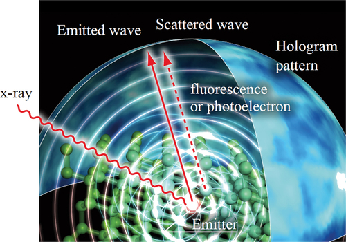
Atomic resolution holography [Citation8] is an evolution of these methods. The principle of atomic resolution holography is shown in . There are two kinds of measurement methods, normal mode and inverse mode as shown in ), respectively. In the normal mode, when X-rays are irradiated to the sample, core-level photoelectrons or fluorescent x-rays are emitted from the atoms in the sample. It spreads as a spherical wave and is scattered by the surrounding atoms. The scattered waves interfere with the unscattered wave. Interference fringes appear in the intensity angular distribution. Since this interference fringe has the property of a hologram, it is possible to reconstruct the atomic structure around the atom emitting the wave without an initial model. By selecting the kinetic energy of specific photoelectrons or the energy of fluorescent X-ray, it is possible to measure the atomic arrangement around the aimed element.
Figure 1. (a) Principle diagram of normal mode of atomic resolution holography. (b) Principle diagram of inverse mode.

Atomic resolution holography gives information beyond LEED and X-ray crystal structure analysis, which utilize the periodicity of atomic arrangement. They are powerful methods but the obtained atomic structure is limited in a unit cell. Therefore, it is impossible to observe non-periodic structure such as the dopant, the adsorbate, or the non-periodic structural distortion. Atomic resolution holography does not require a periodic structure in principle and can measure the non-periodic atomic structure, such as dopants [Citation29–31] and non-periodic crystal structure distortion [Citation32].
It is possible to improve the accuracy of the 3D atomic image by measuring multi-energy holograms [Citation33]. In the case of photoelectron holography, it is possible to measure multi-energy hologram by changing the energy of incident light. However, since the photon energy of x-ray fluorescence is fixed, wavelength cannot be changed. Therefore, the inverse mode shown in is used. When x-rays are incident on the sample, the incident wave is scattered by the atoms and interferes with the direct wave to generate a atomic-scale density distribution. This density distribution is modulated by the incident direction of X-rays. Since the intensity of the fluorescence is in proportion to this modulation, the intensity oscillation depending on the incident angles forms a hologram. This can be regarded as time reversal of the normal mode. In addition, there are some inverse mode methods with using electrons [Citation34] and neutron [Citation18].
In order to reconstruct the atomic image from atomic resolution hologram, numerical algorithm is required. Recording process of hologram is important to consider algorithm of atomic image reconstruction calculation. The measured intensity in normal mode is given by
where is the wave function of the excited wave and k is the wave number vector. In the case of photoelectron, various types of waves are excited, so L is an index to distinguish each.
is the wave function of the scattered wave, where a is the position vector of the scatterer atom, and j is the index of the scatterer atom. Since the hologram is represented by subtracting the intensity of the reference wave and the interference intensity of the direct wave is dominant, the hologram is given by
The hologram represents the sum of the scattering pattern function given by each atom. In the case of electrons, the scattering process is potential scattering and in the case of fluorescent x-rays it is Thomson scattering. The scattering processes are different, but the wave function of the scattered wave is generally expressed as follows,
where is the scattering amplitude. The scattering pattern function
is shown in . We used the partial wave expansion method to calculate the scattered wave of the electron [Citation35]. In the case of s-wave photoelectron as shown in ), since atoms play a role of an electrostatic lens, a forward focusing peak (FFP) appears in the direction of the scatterer. In addition, interference rings are formed around it. When the scatterer atom is located farther away, the number of the interference ring increases (). Therefore, FFP and the center of the interference rings represent the direction of the scatterer atom, and the number of the rings represents the atomic distance. ) show the case of p core-level photoelectron excited by unpolarized light. In the light direction, hologram pattern disappears. show LMM Auger electron. In this case, f-wave is mainly emitted, and pattern is different from ). Therefore, because of the phase shift effect and asymmetric emitted wave, the intensity modulation cannot be represented by a simple trigonometric function. shows the simulation result of the photoelectron hologram comparing with the experimental result. In this calculation, the effects of multiple scattering was considered.
Figure 2. Examples of scattering pattern functions (SPF), which are the holographic patterns generated by single scatterer atom. (a) SPF of s-wave electron with = 700 eV scattered by an Fe atom located at 0.3 nm. (b) In the case of the 0.6 nm atomic distance. (c), (d) SPF of photoelectron excited from np core-level electron by unpolarized light. (
= 700 eV). (e), (f) LMM Auger electron (f wave) case (
= 700 eV). (g) In the case of XFH.
= 10 keV.

Figure 3. Comparison of simulated photoelectron hologram and photoelectron hologram measured on Si(001) surface with Sienta Omicron DA 30 [Citation29]. Left side is the experimental hologram of photoelectrons excited from 2p core-level electron by unpolarized light ( = 600 eV). Right side is simulation using atomic cluster with 2nm-radius and 1nm mean free path.
![Figure 3. Comparison of simulated photoelectron hologram and photoelectron hologram measured on Si(001) surface with Sienta Omicron DA 30 [Citation29]. Left side is the experimental hologram of photoelectrons excited from 2p core-level electron by unpolarized light (Ek = 600 eV). Right side is simulation using atomic cluster with 2nm-radius and 1nm mean free path.](/cms/asset/6581645c-e478-4f37-af82-f8c0b9cf5837/tapx_a_2350161_f0003_oc.jpg)
) shows the case of X-ray fluorescence hologram. The center of the interference ring represents the direction of the scatterer atom, and the number of interference fringes represents the atomic distance. The scattering amplitude reduction at backscattering is due to the atomic structure factor. In the case of x-ray fluorescence, the phase anisotropy of the direct wave is negligible, so the pattern can be represented by a simple trigonometric function.
To obtain atomic images from the hologram, a method based on Fourier transform was proposed at an early stage [Citation10]. This can be applied to x-ray fluorescence holography because of small phase-anisotropy anisotropy and no strong FFP. In the Fourier transform, the amount of information is preserved before and after the conversion. Therefore, in order to reconstruct the image of the 3D volume by this method, it is necessary to measure the hologram in 3D. For this reason, the inverse mode of X-ray fluorescence holography, which can record the volume hologram using photon energy tunable light source, is mainly used.
On the other hand, in the case of photoelectrons, Fourier transform cannot be applied due to the large anisotropy of the phase of direct wave and the existence of strong FFP [Citation36,Citation37]. Therefore, we developed an algorithm based on the fitting method using scattering pattern function. By using the maximum entropy method [Citation38,Citation39] and sparse modeling [Citation40], image reconstruction is possible even with one hologram.
The error function of this fitting is defined as follows.
Here, represents the hologram obtained by the measurement, and
is the atomic distribution function. The atomic distribution function may be determined by minimizing this error function. However, the number of the unknown parameters is much more than the number of the known values. When hologram is measured in steps of 1°, the number of the known values are about 41,000 points. When the atomic distribution function is defined within ±1 nm cubic regions with 0.01 nm steps, the number of the unknown value becomes 8 million. In order to solve it, the sparse modeling (Lasso) is effective because this atomic distribution function does not take a negative value and mostly takes a value of zero. The corrected error function by Lasso is expressed below.
where λ is a parameter that controls sparseness, and as it is larger, a sparse solution is obtained. This parameter should be treated carefully [Citation40]. This calculation method can be applied to all atomic resolution holography. In addition, if the translational symmetry manipulation is permitted, applying a translational symmetry operation to the voxel yields a very clear atomic image [Citation19]. shows the atomic image obtained from one experimental photoelectron hologram of . A 3D atomic image is obtained with high accuracy.
Figure 4. (a) The atomic arrangement of Si reconstructed from the experimental hologram of . (b) Since there are two equivalent atomic sites in the Si unit cell, the reconstructed atomic image is a superposition of atomic images seen from the two sites.

3. Experiment of photoelectron holography
Direct visualization of three-dimensional (3D) atomic arrangements around specific atomic sites of functional materials is essential to clarify the mechanism of various electronic properties. Photoelectron diffraction and holography as an element selective local structure analysis method is adequate for this purpose [Citation41–48]. Here, two examples of photoelectron holography (PEH) technique applied to local structure analysis of dopant and intercalant atoms are introduced.
As mentioned in the introduction section, atomic-level characterization of dopant atoms in silicon devices was an unsolved yet important issue. Since the PEH is an element-specific method for the local 3D atomic structures even without translational symmetry, Tsutsui et al. applied this method to the system of arsenic (As) atoms doped p-type Si(001) surface [Citation29]. Measurements were done at BL25SU of SPring-8. The circularly-polarized soft x-ray (left and right) was incident onto the sample with a glancing angle of 85° from the sample surface normal axis. The substrate and dopant atom-specific core-level photoelectron angular distributions were measured by a hemispherical electron analyzer (Scienta Omicron DA30). The full hemispherical photoelectron holograms were acquired by stepwise variation of the photoemission angle θ and the sample azimuthal angle φ rotations. The As concentration was ~1.5 × 1020 cm−3. The As 3d photoelectron spectrum indicated possible three components with high-, middle-, and low-binding energies named BEH, BEM, and BEL components at small, middle, and large kinetic energies, respectively, as shown in . The hologram for the BEH peak is significantly clear and rather similar to that of the Si 2p hologram () indicating that the As atoms corresponding to the BEH are located at the substitutional site in the Si lattice. Forward focusing peaks corresponding to the second nearest neighbor atom directions at <110> are noticeably stronger than the forward focusing peaks along the first nearest neighbor atom directions at <111> (). In the reconstructed atomic images, the first nearest neighbor atom is quite weak () in comparison with the Si case for z = 0.135 nm. This agreed with the complementary molecular dynamics simulations concluding that the first nearest neighbor Si atoms from the As atom are fluctuating significantly compared with the second nearest neighbor Si atoms as schematically shown in ). In the hologram for the BEM peak, intensity of the hologram is generally much weaker than the case of BEH case, whereas the Kikuchi-lines are evident and the forward focusing peaks at <111> directions are still recognizable ()). In the case of the As atom corresponding to the BEM (not shown), the atomic images of the first nearest neighbor atoms at (1/4,1/4,1/4) are visible at z = 0.135 nm, while the reconstructed atomic images at (1/2,1/2,0) at z = 0 nm were very elongated. Multiple As atoms occupy the Si substitutional sites associated with a Si vacancy AsnV (n = 2–4) are the candidate for the BEM peak. Holographic pattern is much obscured in the case of BEL ()). One can imagine that the As atoms corresponding to the BEL are located either in the amorphous or disordered environment or precipitated Si-As region. Among these, As dopants responsible for the BEH peak are electrically active and those for the BEM and BEL are not. The local atomic arrangements of As determined on the basis of holograms with the different binding energy shifts were successfully associated with their electric properties. Spectro-photoelectron holography is now regarded as a powerful approach to investigate the dopant science.
Figure 5. Holograms generated from the spectra labeled (a) BEH, (b) BEM, and (c) BEL, and (d) as 3d core-level photoelectron spectra with labels. After ref [Citation29].
![Figure 5. Holograms generated from the spectra labeled (a) BEH, (b) BEM, and (c) BEL, and (d) as 3d core-level photoelectron spectra with labels. After ref [Citation29].](/cms/asset/7f2b00e4-b941-4b9e-a828-bb45020d1993/tapx_a_2350161_f0005_oc.jpg)
Figure 6. Atomic images reconstructed from the hologram of each atomic site. The corresponding BEH spectrum and hologram are shown in ). The cross sectional images are labeled as z = (a) 0, (b) 0.135 (= a/4), and (c) 0.27 nm (= a/2). The candidate structure is shown in (d). After ref [Citation29].
![Figure 6. Atomic images reconstructed from the hologram of each atomic site. The corresponding BEH spectrum and hologram are shown in Figure 5(d,a). The cross sectional images are labeled as z = (a) 0, (b) 0.135 (= a/4), and (c) 0.27 nm (= a/2). The candidate structure is shown in (d). After ref [Citation29].](/cms/asset/f64994d9-4244-4e60-89fc-907cf8560ffa/tapx_a_2350161_f0006_oc.jpg)
This PEH technique was also applied to the structure analysis of (Ca,K)C8, superconductor (Tc = 9.9 K). The photoelectron spectra of the cleaved surface of (Ca,K)C8 showed only C 1s and K 2p peaks, and the Ca 2p peak intensity was less than a few hundredths of that of the K 2p peak. The observation of the K dominant structure at the cleaved surface implies that Ca atoms are dispersed in the bulk and likely form high Tc domains. ) show full hemisphere C 1s and K 2p photoelectron holograms at the kinetic energy of 600 eV [Citation49]. The incidence direction of soft x-ray was aligned along the surface normal. From these holograms, atomic images from the few-layer region of cleaved surface were directly reconstructed. The PEH reconstruction algorithm, SPEA-MEM, a fitting-based approach of diffraction rings and FFPs by simulated data under maximum entropy method scheme [Citation19–21] were applied. Graphene atomic images were collected in the in-plane cross sections of the layers 3.3 Å and 5.7 Å above the photoelectron emitting C atom as shown in ). Note that some of the reconstructed spots have strong intensities. Schematic diagrams in ) explain how the different stacking registries result the modulation in the reconstructed atomic image intensity. The ‘B’ layer can be stacked on the ‘A’ layer with a translational shift equal to the CC bond length in the CC bond direction as shown in , or the ‘B’ layer can be stacked with a translational shift in the opposite direction, as shown in . For the layer stacked in the AA () and AB ()) sequences, bright spots form triangular and hexagonal lattices, respectively. The stacking structures for the layers 3.3 Å and 5.7 Å above were determined as AB- and AA-type, respectively. The intercalant metal atom layer was found between two AA-stacked graphenes. The K atomic image revealing 2 × 2 periodicity, occupying every second center site of C hexagonal columns, was reconstructed as shown in .
Figure 7. (a) C 1s and (b) K 2p photoelectron intensity angular distributions (holograms) from (Ca,K)Cy. After ref [Citation49].
![Figure 7. (a) C 1s and (b) K 2p photoelectron intensity angular distributions (holograms) from (Ca,K)Cy. After ref [Citation49].](/cms/asset/5bba2e93-9455-4ec9-93ae-616d0db18c2a/tapx_a_2350161_f0007_oc.jpg)
Figure 8. (a) Reconstructed atomic arrangement image at (a) z=3.3 and (b) 5.7 Å. Atomic configuration models of (c) AA, (d) AB, and (e) AB’ bilayer stacking structures. Graphene clusters can be stacked on top of the A graphene layer in three different ways. (f)–(i) the schematic structure model in each stacking geometry and the expected signal intensity ratio at the centre; the first- and the second-neighbouring atoms in the reconstructed real space images. After ref [Citation49].
![Figure 8. (a) Reconstructed atomic arrangement image at (a) z=3.3 and (b) 5.7 Å. Atomic configuration models of (c) AA, (d) AB, and (e) AB’ bilayer stacking structures. Graphene clusters can be stacked on top of the A graphene layer in three different ways. (f)–(i) the schematic structure model in each stacking geometry and the expected signal intensity ratio at the centre; the first- and the second-neighbouring atoms in the reconstructed real space images. After ref [Citation49].](/cms/asset/1fd942cc-4d18-4026-8c05-1923e322d215/tapx_a_2350161_f0008_oc.jpg)
Figure 9. (a) Atomic arrangement image of C (blue) and K (orange) layers. (b) Structure model of the cleaved surface region of (Ca,K)Cy. After ref [Citation49].
![Figure 9. (a) Atomic arrangement image of C (blue) and K (orange) layers. (b) Structure model of the cleaved surface region of (Ca,K)Cy. After ref [Citation49].](/cms/asset/537c549a-86c5-494d-9e47-f68d7230018c/tapx_a_2350161_f0009_oc.jpg)
These observations revealed that the cleavage preferentially occurs at the K atom intercalated layers containing no Ca atoms, which is likely the most fragile part of the crystal sample. The most important result from the present study is that the cleaved surface does not always represent the averaged bulk structure. The structure and composition of the surface and the bulk can be substantially different, especially in a layered system. Special attention must be paid when using surface-sensitive methods, such as ultraviolet photoelectron spectroscopy and scanning probe microscopy.
As described above, photoelectrons from the localized core levels are excellent probes for element-specific atomic structure analysis. Since diffraction patterns differ according to the atomic arrangements surrounding excited atomic sites, such atomic-site-specific information can be ‘fingerprinted’ by their characteristic diffraction patterns. These diffraction patterns, combined with spectroscopy, can be used as atom-site resolution probes for local electronic structure investigations [Citation50–53]. By using a focused soft-x-ray beam together with a sample scanning mechanism and a display-type spherical mirror analyzer (DIANA) [Citation54,Citation55] as an efficient photoelectron angular distribution imaging device, scanning microscopic photoelectron diffraction measurement is realized. The electronic, chemical, and magnetic properties of domains with different surface orientations of polycrystalline sample were characterized by combining diffraction measurements with X-ray absorption spectroscopy techniques [Citation56,Citation57].
4. X-ray fluorescence and neutron holography
Most of crystal structures can be determined by diffraction techniques. However, in principle, they are not applicable to characterizations of dopants in materials because they need periodicity of atomic arrangements. X-ray absorption fine structure (XAFS) can analyze local structures around dopants. Although many researchers use XAFS nowadays, they can obtain only radial distribution functions around target elements. In this context, x-ray fluorescence holography (XFH) [Citation16,Citation58] and neutron holography (NH) [Citation17,Citation59,Citation60] can provide 3D atomic images around target elements, which are more informative than the radial distribution function.
There are two modes of XFH and NH: normal and inverse modes as shown in . However, here we limit the discussion to the inverse mode [Citation61], because most of the experiments have been carried out using the inverse mode. In this scheme, target elements are needed to emit secondary radiations, such as fluorescent x-rays or γ-rays. The unscattered radiation from x-ray and neutron sources play a role of the holographic reference waves R. The scattered radiations by individual atoms are treated as the object waves O. The interference between reference and object waves is probed directly at the sites of absorbing atoms (the so-called atomic detectors) by measuring the fluorescence yield with an external detector. The hologram is collected by rotating the sample relative to the direction of the incident beam.
To date, XFH are applied to many materials, such as ferroelectrics [Citation62], ferromagnetic semiconductors [Citation63,Citation64], topological insulators [Citation30,Citation65]. Here, among many applications we introduce our XFH result of a Mg alloy including transition metal clusters [Citation66,Citation67], which show an excellent mechanical property, incombustibility and a curious microscopic structure, the so-called ‘long-period stacking ordered’ (LPSO) structure [Citation68]. Although the excellent mechanical property is believed to be associated with the LPSO structure, its mechanism has not been fully understood so far. Therefore, we investigated the role of the transition metal clusters in the Mg alloy by measuring XFH hologram of Mg75Zn10Y15 at the beamline BL39XU at synchrotron radiation facility of SPring-8.
The polycrystalline sample was supplied by Hagihara laboratory at Osaka University [Citation69]. Although polycrystalline samples are hardly applicable to XFH measurement in principle, LSPO structure Mg alloys include sub-millimeter grains. We focused the incident x-ray beam to 20 × 20 μm2 using a focusing mirror and slits at BL39XU, and irradiated it on one large grain with the size of 0.3 × 1.0 mm2. Zn Kα fluorescent x-rays from the sample were selected by a cylindrical graphite analyzer and were detected by avalanche photodiode. The XFH measurements were carried out by recording the x-ray fluorescence intensity variation as a function of the direction of the incident x-rays. To obtain accurate atomic images, we recorded 15 holograms with different incident x-ray energies from 10.0 to 13.5 keV in steps of 0.25 keV.
shows Zn Kα hologram recorded at 10.0 keV. We can observe clear standing wave lines, confirming that the measurements were successfully performed. Barton algorithm [Citation33], which is similar to Fourier transformation, was applied to the holograms to reconstruct atomic images. shows the experimental and calculated in-plane atomic images around Zn. For Mg75Zn10Y15, existence of Zn6Y8 clusters () were confirmed using transmission electron microscope (TEM) [Citation70]. The neighbor strong images indicated by solid circles in the experimental reconstruction correspond to Zn–Zn correlation within the Zn6Y8 cluster, which evidences the formation of the robust clusters. On the other hand, the atomic images corresponding to the Zn atoms outside the cluster are hardly observed (dashed circles), which indicates the weak inter-cluster positional correlations. The experimental results are well reproduced by the calculations including the positional fluctuations of the Zn6Y8 clusters, that is, the strong atomic images observed at the positions of dashed circles (lower right in become considerably weaker by introducing the positional fluctuations (lower left in . Based on this calculation, we evaluated the magnitude of the fluctuations to be more than ±0.33 Å. Because the degree of order is strongly related to the mechanical properties, the quantitative information of the inter-cluster fluctuation will be useful for understanding the origin of the excellent mechanical properties of LPSO alloys.
Figure 10. Hologram of Mg75Zn10Y15 and the reconstruction of Zn6Y8 cluster. (a) Zn Kα hologram taken at 10.0 keV. (b) Atomic images around Zn at z = 0.0 Å. The upper and lower images are obtained from the experimental and simulated holograms, respectively. (c): Model of Zn6Y8 cluster. After ref [Citation67].
![Figure 10. Hologram of Mg75Zn10Y15 and the reconstruction of Zn6Y8 cluster. (a) Zn Kα hologram taken at 10.0 keV. (b) Atomic images around Zn at z = 0.0 Å. The upper and lower images are obtained from the experimental and simulated holograms, respectively. (c): Model of Zn6Y8 cluster. After ref [Citation67].](/cms/asset/1220fc17-9a35-4a13-ab23-1fe3a9e069dd/tapx_a_2350161_f0010_oc.jpg)
Although XFH has used for a lot of unknown local structures in advanced materials, the number of NH applications is small. One of the strong reasons for this is single wavelength recording [Citation71] due to the weakness of a monochromatic neutron beam whose flux is typically six orders of magnitude smaller than that of an x-ray beam from a third-generation synchrotron radiation source. From the experiences of XFH experiments, it is known that visibility of the atomic images is drastically improved using multiple-wavelength recording of holograms. In this context, we successfully demonstrated multiple-wavelength neutron holography using the time-of-flight (TOF) technique with pulsed neutrons at spallation neutron source facility of J-PARC [Citation18,Citation72].
The measured sample for this demonstration is a 1 at.% Eu-doped CaF2 single crystal. Eu nuclei in the sample used in this study emit γ-rays upon absorbing neutrons rather than other elements of Ca and F. Therefore, Eu atoms become a good target element for recording holograms in inverse mode. The neutron wavelength, λ, which is inversely proportional to the neutron velocity, is obtained from the time of flight from the spallation source to the sample. shows the TOF spectrum of the γ-ray intensity. Multiple-wavelength neutron holograms can be obtained by measuring the angular variation of γ-ray intensity at each TOF. shows the multiple-wavelength hologram obtained by superimposing holograms for 34 different wavelengths along the radial direction.
Figure 11. Multiple-wavelength hologram of Eu-doped CaF2 and 3D atomic images around Eu. (a) TOF spectrum of γ-ray intensity from Eu. (b) Superimpose of 34 different wavelength holograms. 3D images obtained from (c) Experimental and (d) Calculated holograms. After ref [Citation18].
![Figure 11. Multiple-wavelength hologram of Eu-doped CaF2 and 3D atomic images around Eu. (a) TOF spectrum of γ-ray intensity from Eu. (b) Superimpose of 34 different wavelength holograms. 3D images obtained from (c) Experimental and (d) Calculated holograms. After ref [Citation18].](/cms/asset/db1e14bb-22db-494e-921e-75f4782e5466/tapx_a_2350161_f0011_oc.jpg)
From the volume hologram, we successfully reconstructed a real-space image around Eu using the Barton multiple-wavelength reconstruction algorithm [Citation33]. The images in ) are experimentally and theoretically reconstructed atomic images, respectively. The theoretical reconstruction was obtained from the calculated holograms using a model in which Eu atoms substitute for Ca without distortion of surrounding lattice. Comparing the two real-space images, we found a significant difference at the nearest Ca positions. These Ca atomic images are split into two parts. This indicates large displacements of the Ca atoms from the ideal positions, which was also observed by X-ray absorption fine structure (XAFS). Moreover, XAFS indicated that trivalent Eu substituting for divalent Ca, suggesting that this gave rise to an interesting feature of the local structure that allows it to maintain charge neutrality.
Here, perspectives of XFH and NH are described. XFH and NH need single crystals in principle, and thus, this restricts the number of applications. In particular, a ceramic, whose grain sizes are typically of the order of micron meter, is one of the important samples that we must apply. Therefore, we plan to construct a new XFH setup using a focused X-ray beam with the size of less than 1 μm. Another direction of XFH is valence selective measurement using resonant excitations at the absorption edges of different valences. On the other hand, since the multi-wavelength NH is a quite new method, it will be applied to many interesting samples in future. In particular, NH is promising for local structure analyses of light elements and magnetic moments [Citation73].
5. Surface x-ray holography
X-ray scattering amplitude F(Q) is proportional to the Fourier transform of the electron density ρ(r). In case of crystals, which involve repetition in space by definition, the three-dimensional lattice gives rise to Bragg peaks at the reciprocal lattice points. The relative intensity of the Bragg peaks reflects the internal structure of the unit cell. When the crystal has a flat surface, the electron density has a sharp termination. The total electron density can be expressed as ρcry(r) Θ(z), where ρcry(r) and Θ(z) denote the electron density of the ideal crystal having infinite volume and the Heaviside step function, respectively. The Fourier transform of ρcry(r) Θ(z) is a convolution of the Fourier transform of ρcry(r) and Θ(z). The former gives Bragg peaks, and the latter gives rod-shaped intensity distribution perpendicular to the surface; convolution of them results in a rod-shaped tail from each Bragg reflection. Such intensity distribution is called crystal truncation rod (CTR) scattering [Citation74,Citation75].
In order to clarify the electron density distribution around the surface, we can use the CTR scattering. A simple inverse Fourier transform of the CTR scattering amplitude provides the electron density around the surface. However, as is well known as the phase problem, it is impossible to measure the phase of the amplitude. We need to have some trick to obtain the phase information. The CTR scattering amplitude from a real surface can be written as a sum of the scattering amplitude from the ideal surface Fi(Q) and that from the structural modulation Fu(Q) caused by the surface. It is easy to calculate Fi(Q) because the bulk crystal structure is known. Therefore, we can use Fi(Q) as the reference wave of the holography to obtain Fu(Q). There are several ways to derive Fu(Q) from measured intensity and the calculated Fi(Q) [Citation22,Citation76].
There are vast number of structural studies on various surface or interface-related phenomena, such as electrochemical reactions [Citation77–79], photocatalytic activities [Citation80,Citation81], electric double-layer formation [Citation82,Citation83], and organic semiconductor-based electronic device activities [Citation84–87]. The CTR scattering profiles of these molecules are shown in . In recent years, interfaces of transition metal oxides [Citation88–94] and topological insulators [Citation95] attracted much attention. Here, we will focus our attention on organic semiconductor devices.
Figure 12. CTR scattering profiles of [n]phenacenes (n = 5, 7 and 9), tetracene, and rubrene single crystals. The unit for the horizontal axis is the length of the c* except for rubrene. For rubrene, the unit was chosen to 2c* as the unit cell contains two layers of molecules [Citation85,Citation86].
![Figure 12. CTR scattering profiles of [n]phenacenes (n = 5, 7 and 9), tetracene, and rubrene single crystals. The unit for the horizontal axis is the length of the c* except for rubrene. For rubrene, the unit was chosen to 2c* as the unit cell contains two layers of molecules [Citation85,Citation86].](/cms/asset/8556d103-7c5a-4814-81c2-a0278d120b2f/tapx_a_2350161_f0012_oc.jpg)
Organic semiconductor devices have been studied in the past few decades [Citation96]. The most popular ones are organic electroluminescence displays, followed by the solar cells. The simplest form of the organic devices is the field effect transistors (FETs). The carrier conduction in the organic FET happens at the interfacial several molecular layers [Citation97]. The transfer integral in the organic semiconductors depends on the overlap integral between the neighboring molecules, which is highly affected by the molecular arrangements. In addition, the carrier conduction mechanism in organic semiconductors [Citation98] is very different from that in doped Si, and therefore, the knowledge of the molecular arrangement at the interface is needed to understand the physics of organic FETs.
Although there have been several CTR measurements reported on organic crystals [Citation99], the electron density as a function of depth had never been reported until 2010 [Citation84]. Until now, the depth profile of the electron density of rubrene, tetracene, and [n]phenacenes are reported. Rubrene and tetracene have similar highest occupied molecular orbitals (HOMO), while the crystal structures of them are very different as can be seen in . Tetracene has a straight arrangement of the six-membered rings, and phenacenes have a zig-zag arrangement of them. The molecular packing of tetracene and phenacenes are common, so-called herringbone packing. Among them, tetracene has significantly small carrier mobility. In the phenacene series, the mobility gradually increases as n increases.
Figure 13. (a) Crystal structure of (left) tetracene and (right) rubrene. The size of the unit cells are shown by the solid line. The molecular packing of phenacenes is similar to that of tetracene. (b)-(f) Electron density profiles for [n]phenacenes, tetracene, and rubrene as a function of depth derived by the coherent bragg rod analysis method. Those for the ideal surfaces (surfaces having no relaxation) are also presented by the red curves [Citation85,Citation86].
![Figure 13. (a) Crystal structure of (left) tetracene and (right) rubrene. The size of the unit cells are shown by the solid line. The molecular packing of phenacenes is similar to that of tetracene. (b)-(f) Electron density profiles for [n]phenacenes, tetracene, and rubrene as a function of depth derived by the coherent bragg rod analysis method. Those for the ideal surfaces (surfaces having no relaxation) are also presented by the red curves [Citation85,Citation86].](/cms/asset/a1f66e08-bf78-44ec-96cb-a5bd4067dfa7/tapx_a_2350161_f0013_oc.jpg)
In order to measure the depth profiles of electron density for the crystals whose surface is parallel to the c-plane, the CTR intensity profile along the (00 l)-rod is needed. shows the measured intensity profiles for rubrene, tetracene, and [n]phenacenes [Citation85,Citation86]. Sharp peaks at integer l positions are the Bragg peaks, and the intensity distribution in the middle of them are the CTR scattering. Calculated profiles based on the reported single crystal structures (rubrene, tetracene and [5]phenacene) and on the structure derived from the first principle calculations ([7] and [9]phenacenes) are also presented by the red curves. Most of the calculated profiles well reproduce the experimental results. ) shows the electron density profiles of them derived by the coherent Bragg rod analysis [Citation76]. As can be seen, internal structure of molecule is observed. In most cases, the surface layer has the same electron density as that of the inside layers. One exception is tetracene, whose first layer is apparently different from other layers, indicating that there is a strong surface relaxation.
The transfer integrals between the molecules are calculated from the molecular arrangement. The first principle calculations based on the surface relaxation observed in tetracene derive very different band structure from the bulk structure, and much smaller transfer integrals [Citation85]. Photoelectron spectroscopy [Citation100] shows clear band dispersion in rubrene in agreement with the theoretical prediction [Citation101], whereas only a broad and flat signal was observed in tetracene. While this difference was attributed to the effect of phonon or to the surface disorder in ref. [Citation100], it can also be explained by the large surface relaxation that was not taken into account in their study.
The electron density profiles of organic semiconductors commonly have negligible amount of modulation in the second molecular layer or deeper; the surface effect on the structure is limited to the first molecular layer, if any. This common feature of the surface relaxation in organic semiconductors is explained by the weak inter-molecular interaction between the layers. The effect of the missing of a layer can cause some deformation to the first monolayer, while the effect cannot cause noticeable change in the second neighbors.
6. Stereography of atomic arrangement
The above mentioned holographies are direct structure analysis methods because it does not require prior structure models for the analysis. However, they still require calculations and the resulting structures cannot be imagined from the hologram. A more direct method of stereophotography [Citation23] has been developed, where one can view the 3D atomic arrangement directly with eyes.
This method utilizes the orbital angular momentum of photoelectrons around the emitter atom. When a photoelectron is excited by a circularly polarized light, the angular momentum of the circularly polarized photon (±1ћ) is transferred to the photoelectron. It was found that when the photoelectron has an orbital angular momentum the forward focusing peaks (FFP in in section 2) rotate in the same direction of the circularly polarized light [Citation102]. The rotation angle of FFP is inversely proportional to the distance between the emitter and the scatterer atoms. This relation is the same as parallax which is the origin when we recognize three-dimensional arrangement. Hence, stereophotograph of atomic arrangement can be obtained. Several stereophotpgraphs have been obtained so far [Citation41,Citation103,Citation104].
) are stereophotographs of atomic arrangement of InP crystal [Citation103]. These photographs are the scenery viewed from an In atom to nearest neighbor P atom along [111] direction. When you see with your left eye and with your right eye, the atom A (nearest P atom) looks closer to you than the atoms B and C (second nearest In atoms). ) are actually a two-dimensional photoelectron angular distribution patterns taken by a display-type spherical mirror analyzer DIANA [Citation54,Citation55] excited by counter-clockwise and clockwise circularly polarized soft x-rays. Because the angle between the center ([111] direction) and the atom B ([110] direction) is 35.3° which is much smaller than the acceptance angle of DIANA (±60°) these patterns are displayed on the screen of DIANA at once.
Figure 14. (a) and (b) are stereophotographs of atomic arrangement of InP crystal viewed from the emitter In atom O. (a) Is for left eye and (b) for right eye. (c) Propagating direction of photoelectrons excited by counter-clockwise (red) and clockwise (blue) circularly polarized light. After ref. [Citation103].
![Figure 14. (a) and (b) are stereophotographs of atomic arrangement of InP crystal viewed from the emitter In atom O. (a) Is for left eye and (b) for right eye. (c) Propagating direction of photoelectrons excited by counter-clockwise (red) and clockwise (blue) circularly polarized light. After ref. [Citation103].](/cms/asset/5a15c4d7-498f-423e-9e54-39910e3a7974/tapx_a_2350161_f0014_oc.jpg)
The orbital angular momentum is a product of the momentum and the impact parameter b which is a distance between the trajectory and the emitter nuclei. Hence, the trajectory of particles having orbital angular momentum does not start from the center of the emitter atom but start at a point on the circle of radius b as shown in . This explanation is made by classical mechanics, but the result is the same as that of wave dynamics [Citation102]. Red (blue) arrows show the trajectory of photoelectrons excited by counter-clockwise (clockwise) circularly polarized light, which show the direction of FFP from the scatterer atoms. Hence, the angular shifts between red and blue arrows are the same as the parallax of the FFP in ) which correspond to the parallax seen from the left eye at L and right eye at R in . Hence, we can recognize the three-dimensional atomic arrangement directly in our brain when we see the stereophotographs ) by our left and right eyes, respectively.
7. Conclusions and outlook
This article reviewed the principles of atomic-resolution holographies and several results obtained by the project ‘3D Active-Site Science’. 3D local atomic structures around specific active-site atoms with no translational symmetry in functional materials have been revealed for the first time. Because the standard structure analysis method of x-ray diffraction (XRD) cannot study these local active-sites which have no translational symmetry, this success opened a new era to study the mechanism of functional materials from local 3D atomic structure of active centers. We hope many readers of this article start to use atomic-resolution holographies to develop new functional materials from atomic point of view.
At present, these techniques of atomic-resolultion holography requires synchrotron radiation, which can be used only in synchrotron radiation facilities. Hence, it is hoped to develop an apparatus to observe atomic-resolultion holography at any laboratories.
Acknowledgments
This research was supported by JSPS under Grant-in-Aid for Scientific Research on Innovative Areas “3D Active-Site Science” Nos. 26105001, 26105007, 26105013. JSPS Grant-in-Aid for Transformative Research Areas “Hyper-ordered Structures Science” Nos. 20H05878, 20H05881, 20H05882, 23H04122.
Disclosure statement
No potential conflict of interest was reported by the author(s).
References
- Deguchi H, Yoshida H, Inagaki T, et al. EXAFS study of doped ceria using multiple data set fit. Solid State Ion. 2005;176:1817–1825. doi: 10.1016/j.ssi.2005.04.043
- Kompch A, Sahu A, Notthoff C, et al. Localization of Ag dopant atoms in CdSe nanocrystals by reverse monte carlo analysis of EXAFS spectra. J Phys Chem C. 2015;119:18762–18772. doi: 10.1021/acs.jpcc.5b04399
- Kraynis O, Timoshenko J, Huang J, et al. Modeling strain distribution at the atomic level in doped ceria films with extended X-ray absorption fine structure spectroscopy. Inorg Chem. 2019;58:7527–7536. doi: 10.1021/acs.inorgchem.9b00730
- Kluherz KT, Mergelsberg ST, Sommer DE, et al. Defect structure in quantum-cutting Yb3+-Doped CsPbCl3 perovskites probed by X-Ray absorption and atomic pair distribution function analysis. Phys Rev Mater. 2022;6:074601. doi: 10.1103/PhysRevMaterials.6.074601
- Gurman SJ, McGreevy RL. Reverse monte carlo simulation for the analysis of EXAFS data. J Phys Cond Matter. 1990;2:9463–9473. doi: 10.1088/0953-8984/2/48/001
- Keen DA, McGreevy RL, Hayes W, et al. Structural disorder in AgBr: reverse monte carlo analysis of powder neutron-diffraction data. Philos Mag Lett. 1990;61:349. doi: 10.1080/09500839008206504
- Daimon H. Atomic-resolution holography for active-site structure. Jpn J Appl Phys. 2020;59:010504. doi: 10.7567/1347-4065/ab5f48
- Szöke A. X-ray and electron holography using a local reference beam. In: AIP Conference Proceedings , No.147. New York: AIP; 1986. p. 361.
- Fadley CS, Chen Y, Couch RE, et al. Surface,interface,and nanostructure characterization with photoelectron diffraction and photoelectron and X-ray holography. J Surf Anal. 1997;3:334.
- Barton JJ. Photoelectron Holography. Phys Rev Lett. 1988;61:1356. doi: 10.1103/PhysRevLett.61.1356
- Matsushita T, Muro T, Matsui F, et al. Principle and reconstruction algorithm for atomic-resolution holography. J Phys Soc Jpn. 2018;87:061002. doi: 10.7566/JPSJ.87.061002
- Daimon H. Overview of three-dimensional atomic-resolution holography and imaging techniques: recent advances in local-structure science. J Phys Soc Jpn. 2018;87:061001. doi: 10.7566/JPSJ.87.061001
- Matsui F, Matsushita T, Daimon H. Holographic reconstruction of photoelectron diffraction and its circular dichroism for local structure probing. J Phys Soc Jpn. 2018;87:061004. doi: 10.7566/JPSJ.87.061004
- Faigel G, Bortel G, Fadley CS, et al. Ten Years of x-ray holography. X-Ray Spectrom. 2007;36:3–10. doi: 10.1002/xrs.935
- Hayashi K, Happo N, Hosokawa S, et al. X-ray fluorescence holography. J Phys Condens Matter. 2012;24:093201. doi: 10.1088/0953-8984/24/9/093201
- Hayashi K, Korecki P. X-ray fluorescence holography: principles, apparatus, and applications. J Phys Soc Jpn. 2018;87:061003. doi: 10.7566/JPSJ.87.061003
- Cser L, Krexner G, Török G. Atomic-resolution neutron holography. Europhys Lett. 2001;54:747. doi: 10.1209/epl/i2001-00316-7
- Hayashi K, Ohoyama K, Happo N, et al. Multiple-wavelength neutron holography with pulsed neutrons. Sci Adv. 2017;3:e1700294. doi: 10.1126/sciadv.1700294
- Matsushita T, Guo FZ, Suzuki M, et al. Reconstruction algorithm for atomic-resolution holography using translational symmetry. Phys Rev B. 2008;78:144111. doi: 10.1103/PhysRevB.78.144111
- Matsushita T, Matsui F. Features of atomic images reconstructed from photoelectron, Auger electron, and internal detector electron holography using SPEA-MEM. J Electron Spectrosc Relat Phenom. 2014;195:365. doi:10.1016/j.elspec.2014.05.005
- Matsushita T. Atomic image reconstruction from atomic resolution holography using L1-regularized linear regression. E-J Surf Sci Nanotechnol. 2016;14:158. doi: 10.1380/ejssnt.2016.158
- Takahashi T, Sumitani K, Kusano S. Holographic imaging of surface atoms using surface X-ray diffraction. Surf Sci. 2001;493:36–41. doi: 10.1016/S0039-6028(01)01186-4
- Daimon H. Stereoscopic microscopy of atomic arrangement by circularly polarized-light photoelectron diffraction. Phys Rev Lett. 2001;86:2034. doi: 10.1103/PhysRevLett.86.2034
- JSPS Grant-in-Aid for Scientific Research on Innovative Areas. project number 26105001 3D Active-Site Science. https://www.mext.go.jp/component/a_menu/science/detail/__icsFiles/afieldfile/2015/06/15/1358827_04.pdf https://kaken.nii.ac.jp/ja/grant/KAKENHI-AREA-2604/
- Daimon H, Hayashi K, Kinoshita T, et al. Frontier of active-site science: new insights on material functions. Jpn J Appl Phys. 2020;59. https://iopscience.iop.org/journal/1347-4065/page/Frontier_of_active_site_science
- Daimon H, Sasaki YC, editors. Kinou kouzou kagaku nyu-mon. Tokyo: Maruzen; 2016.
- Daimon H, Sasaki YC, editors. 3D local structure and functionality design of materials. Tokyo: Maruzen and World Scientific; 2019.
- https://sites.google.com/hyperordered.org/3d-air-image
- Tsutsui K, Matsushita T, Natori K, et al. Individual atomic imaging of multiple dopant sites in As-doped Si using spectro-photoelectron holography. Nano Lett. 2017;17:7533. doi: 10.1021/acs.nanolett.7b03467
- Hosokawa S, Stellhorn JR, Matsushita T, et al. Impurity position and lattice distortion in a Mn-doped Bi2Te3 topological insulator investigated by x-ray fluorescence holography and x-ray absorption fine structure. Phys Rev B. 2017;96:214207. doi: 10.1103/PhysRevB.96.214207
- Yokoya T, Terashima K, Takeda A, et al. Asymmetric phosphorus incorporation in homoepitaxial P‐doped (111) diamond revealed by Photoelectron Holography. Nano Lett. 2019;19:5915. doi: 10.1021/acs.nanolett.9b01481
- Hosokawa S, Happo N, Ozaki T, et al. Extent and feature of lattice distortions around Ga impurity atoms in InSb single crystal. Phys Rev B. 2013;87:094104. doi: 10.1103/PhysRevB.87.094104
- Barton JJ. Removing multiple scattering and twin images from holographic images. Phys Rev Lett. 1991;67:3106. doi: 10.1103/PhysRevLett.67.3106
- Uesaka A, Hayashi K, Matsushita T, et al. 3D atomic imaging by internal-detector electron holography. Phys Rev Lett. 2011;107:045502. doi: 10.1103/PhysRevLett.107.045502
- Matsushita T, Matsui F, Daimon H, et al. Photoelectron holography with improved image reconstruction. J Electron Spectrosc Relat Phenom. 2010;178-179:195. doi: 10.1016/j.elspec.2009.06.002
- Len PM, Denlinger JD, Rotenberg E, et al. Holographic atomic images from surface and bulk W(110) photoelectron diffraction data. Phys Rev B. 1999;59:5857. doi: 10.1103/PhysRevB.59.5857
- Takagi H, Daimon H, Palomares FJ, et al. Photoelectron holography analysis of W(1 1 0)(1×1)–O surface. Surf Sci. 2001;470:189. doi: 10.1016/S0039-6028(00)00839-6
- Matsushita T, Yoshigoe A, Agui A. Electron holography: a maximum entropy reconstruction scheme. Europhys Lett. 2005;71:597. doi: 10.1209/epl/i2005-10129-8
- Matsushita T, Guo FZ, Matsui F, et al. Three-dimensional atomic-arrangement reconstruction from an Auger-electron hologram. Phys Rev B. 2007;75:085419. doi: 10.1103/PhysRevB.75.085419
- Matsushita T. Algorithm for atomic resolution holography using modified L1-Regularized linear regression and steepest descent method. Phys Status Solidi B. 2018;255:1800091. doi: 10.1002/pssb.201800091
- Kato Y, Matsui F, Matsushita H, et al. Dopant-site effect in superconducting diamond (111) studied by atomic stereophotography. Appl Phys Lett. 2007;91:251914. doi: 10.1063/1.2824844
- Matsui F, Matsushita T, Daimon H. Photoelectron diffraction and holographic reconstruction of graphite. J Phys Soc Jpn. 2012;81:114604. doi: 10.1143/JPSJ.81.114604
- Maejima N, Matsui F, Matsui H, et al. Site-specific atomic and electronic structure analysis of epitaxial silicon oxynitride thin film on SiC(0001) by photoelectron and Auger Electron Diffractions. J Phys Soc Jpn. 2014;83:044604. doi: 10.7566/JPSJ.83.044604
- Matsui H, Matsui F, Maejima N, et al. Local atomic configuration of graphene, buffer layer, and precursor layer on SiC(0001) by photoelectron diffraction. Surf Sci. 2015;632:98–102. doi: 10.1016/j.susc.2014.09.021
- Maejima N, Horita M, Matsui H, et al. Interfacial atomic site characterization by photoelectron diffraction for 4H-AlN/4H-SiC(11-20) heterojunction. Jpn J Appl Phys. 2016;55:085701. doi: 10.7567/JJAP.55.085701
- Mori D, Oyama Y, Hirose T, et al. Local structural determination of N at SiO2/SiC(0001¯) interfaces by photoelectron diffraction. Appl Phys Lett. 2017;111:201603. doi: 10.1063/1.4997080
- Fukami S, Taguchi M, Adachi Y, et al. Correlation between high gas sensitivity and dopant structure in W-doped ZnO. Phys Rev Appl. 2017;7:064029. doi: 10.1103/PhysRevApplied.7.064029
- Mori D, Fujita Y, Hirose T, et al. Atomic characterization of nano-facet nitridation at SiC (11¯00) surface. Appl Phys Lett. 2018;112:131603. doi: 10.1063/1.5020098
- Matsui F, Eguchi R, Nishiyama S, et al. Photoelectron holographic atomic arrangement imaging of cleaved bimetal-intercalated graphite superconductor surface. Sci Rep. 2016;6:36258. doi: 10.1038/srep36258
- Matsui F, Matsushita T, Kato Y, et al. Atomic-layer resolved magnetic and electronic structure analysis of Ni thin film on a Cu(001) surface by diffraction spectroscopy. Phys Rev Lett. 2008;100:207201. doi: 10.1103/PhysRevLett.100.207201
- Matsui F, Matsushita T, Daimon H. Photoelectron structure factor and diffraction spectroscopy. J Electron Spectrosc Relat Phenom. 2014;195:347. doi:10.1016/j.elspec.2014.02.013
- Matsui F, Fujita M, Ohta T, et al. Selective detection of angular-momentum-polarized auger electrons by atomic stereography. Phys Rev Lett. 2015;114:15501. doi: 10.1103/PhysRevLett.114.015501
- Hashimoto Y, Taguchi M, Fukami S, et al. Site-sensitive X-ray photoelectron spectroscopy of Fe3O4 by photoelectron diffraction. Surf Interface Anal. 2019;51:115–119. doi: 10.1002/sia.6568
- Daimon H. New display-type analyzer for the energy and the angular distribution of charged particles. Rev Sci Instrum. 1988;59:545. doi: 10.1063/1.1139884
- Daimon H, Ino S. Improvement of the spherical mirror analyzer. Rev Sci Instrum. 1990;61:57–60. doi: 10.1063/1.1141923Z
- Matsui F, Yasuda K, Maejima N, et al. Chemical and magnetic properties of polycrystalline iron surface revealed by Auger electron holography, spectroscopy, and microscopy. Jpn J Appl Phys. 2019;58:110602. doi: 10.7567/1347-4065/ab4d37
- Fujita Y, Ota H, Matsushita T, et al. Mapping nanometer and micrometer-scale structures at graphite surface by photoelectron diffraction. Surf Interf Anal. 2019;51:74–78. doi: 10.1002/sia.6551
- Tegze M, Faigel G. X-ray holography with atomic resolution. Nature. 1996;380:49. doi: 10.1038/380049a0
- Sur B, Rogge RB, Hammond RP, et al. Atomic structure holography using thermal neutrons. Nature. 2001;414:525. doi: 10.1038/35107026
- Cser L, Török G, Krexner G, et al. Holographic imaging of atoms using thermal neutrons. Phys Rev Lett. 2002;89:175504. doi: 10.1103/PhysRevLett.89.175504
- Gog T, Len PM, Materlik G, et al. Multiple-energy X-Ray holography: atomic images of hematite (Fe2O3). Phys Rev Lett. 1996;76:3132. doi: 10.1103/PhysRevLett.76.3132
- Hu W, Hayashi K, Ohwada K, et al. Acute and obtuse rhombohedrons in the local structures of relaxor ferroelectric Pb(Mg1/3Nb2/3)O3. Phys Rev B. 2014;89:140103(R. doi: 10.1103/PhysRevB.89.140103
- Hu W, Hayashi K, Fukumura T, et al. Spontaneous formation of suboxidic coordination around Co in ferromagnetic rutile Ti0.95Co0.05O2 film. Appl Phys Lett. 2015;106:222403. doi: 10.1063/1.4921847
- Hayashi K, Uchitomi N, Yamagami K, et al. Large as sublattice distortion in sphalerite ZnSnAs2 thin films revealed by x-ray fluorescence holography. J Appl Phys. 2016;119:125703. doi: 10.1063/1.4945004
- He T, Yang X, Terao T, et al. Pressure-induced superconductivity in AgxBi2−xSe3. Phys Rev B. 2018;97:104503. doi: 10.1103/PhysRevB.97.104503
- Kimura K, Hayashi K, Hagihara K, et al. In-plane positional fluctuations of Zinc Atoms in single crystal Mg85Zn6Y9 alloy studied by X-ray fluorescence holography. Mater Trans. 2017;58:539–542. doi: 10.2320/matertrans.M2016459
- Nishioka T, Yamamoto Y, Kimura K, et al. In-plane positional correlations among dopants in 10H type long period stacking ordered Mg75Zn10Y15 alloy studied by X-ray fluorescence holography. Materialia. 2018;3:256–259. doi: 10.1016/j.mtla.2018.09.002
- Abe E, Kawamura Y, Hayashi K, et al. Long-period ordered structure in a high-strength nanocrystalline Mg-1 at% Zn-2 at% Y alloy studied by atomic-resolution Z-contrast STEM. Acta Mater. 2002;50:3845–3857. doi: 10.1016/S1359-6454(02)00191-X
- Hagihara K, Kinoshita A, Sugino Y, et al. Effect of long-period stacking ordered phase on mechanical properties of Mg97Zn1Y2 extruded alloy. Acta Mater. 2010;58:6282–6293. doi: 10.1016/j.actamat.2010.07.050
- Egusa D, Abe E. The structure of long period stacking/order Mg–zn–RE phases with extended non-stoichiometry ranges. Acta Mater. 2012;60:166–178. doi: 10.1016/j.actamat.2011.09.030
- Hayashi K, Ohoyama K, Orimo S, et al. Neutron holography and diffuse scattering of palladium hydride. Phys Rev B. 2015;91:024102. doi: 10.1103/PhysRevB.91.024102
- Hayashi K, Lederer M, Fukumoto Y, et al. Determination of site occupancy of boron in 6H–SiC by multiple-wavelength neutron holography. Appl Phys Lett. 2022;120:132101. doi: 10.1063/5.0080895
- Szakál A, Markó M, Cser L. Imaging local magnetic structure by polarized neutron holography. Europhys Lett. 2018;122:56001. doi: 10.1209/0295-5075/122/56001
- Andrews SR, Cowley RA. Scattering of X-rays from crystal surfaces. J Phys C. 1985;18:6427. doi: 10.1088/0022-3719/18/35/008
- Robinson IK. Crystal truncation rods and surface roughness. Phys Rev B. 1986;33:3830. doi: 10.1103/PhysRevB.33.3830
- Yacoby Y, Sowwan M, Stern E, et al. Direct determination of epitaxial interface structure in Gd2O3 passivation of GaAs. Nature Mater. 2002;1:99. doi: 10.1038/nmat735
- Ocko BM, Watson GM, Wang J. Structure and electrocompression of electrodeposited iodine monolayers on gold (111). J Phys Chem. 1994;98:897. doi: 10.1021/j100054a026
- Nakamura M. New insights on structural dynamics of electrochemical interface by time-resolved surface X-ray diffraction. Curr Opin Electrochem. 2019;14:200. doi:10.1016/j.coelec.2018.09.001
- Rao RR, Kolb MJ, Halck NB, et al. Towards identifying the active sites on RuO2(110) in catalyzing oxygen evolution. Energy Environ Sci. 2017;10:2626. doi: 10.1039/C7EE02307C
- Shirasawa T, Voegeli W, Arakawa E, et al. Structural change of the Rutile–TiO2(110) surface during the photoinduced wettability conversion. J Phys Chem C. 2016;120:29107. doi: 10.1021/acs.jpcc.6b08448
- Hussain H, Tocci G, Woolcot T, et al. Structure of a model TiO2 photocatalytic interface. Nature Mater. 2017;16:461. doi: 10.1038/nmat4793
- Mezger M, Schroder H, Reichert H, et al. Molecular layering of fluorinated ionic liquids at a charged sapphire (0001) surface. Science. 2008;322:424. doi: 10.1126/science.1164502
- Yamamoto R, Morisaki H, Sakata O, et al. External electric field dependence of the structure of the electric double layer at an ionic liquid/Au interface. Appl Phys Lett. 2012;101:053122. doi: 10.1063/1.4742920
- Wakabayashi Y, Takeya J, Kimura T. Sub-Å resolution electron density analysis of the surface of organic rubrene crystals. Phys Rev Lett. 2010;104:066103. doi: 10.1103/PhysRevLett.104.066103
- Morisaki H, Koretsune T, Hotta C, et al. Large surface relaxation in the organic semiconductor tetracene. Nature Commun. 2014;5:5400. doi: 10.1038/ncomms6400
- Wakabayashi Y, Nakamura M, Sasaki K, et al. Surface structure of organic semiconductor [n]phenacene single crystals. J Am Chem Soc. 2018;140:14046. doi: 10.1021/jacs.8b08811
- Yamamura A, Fujii H, Ogasawara H, et al. Sub-molecular structural relaxation at a physisorbed interface with monolayer organic single-crystal semiconductors. Commun Phys. 2020;3:20. doi: 10.1038/s42005-020-0285-7
- Willmott PR, Pauli SA, Herger R, et al. Structural basis for the conducting interface between LaAlO3 and SrTiO3. Phys Rev Lett. 2007;99:155502. doi: 10.1103/PhysRevLett.99.155502
- Pauli SA, Leake SJ, Delley B, et al. Evolution of the interfacial structure of LaAlO3 on SrTiO3. Phys Rev Lett. 2011;106:036101. doi: 10.1103/PhysRevLett.106.036101
- Yamamoto R, Bell C, Hikita Y, et al. Structural comparison of n-type and p-type LaAlO3/SrTiO3 interfaces. Phys Rev Lett. 2011;107:036104. doi: 10.1103/PhysRevLett.107.036104
- Fong DD, Cionca C, Yacoby Y, et al. Direct structural determination in ultrathin ferroelectric films by analysis of synchrotron x-ray scattering measurements. Phys Rev B. 2005;71:144112. doi: 10.1103/PhysRevB.71.144112
- Fister TT, Zhou H, Luo Z, et al. Octahedral rotations in strained LaAlO3/SrTiO3 (001) heterostructures. APL Mater. 2014;2:021102. doi: 10.1063/1.4865160
- Anada M, Kowa K, Maeda H, et al. Spatial coherence of the insulating phase in quasi-two-dimensional LaNiO3 films. Phys Rev B. 2018;98:014105–1–8. doi: 10.1103/PhysRevB.98.014105
- Nagai K, Anada M, Kowa K, et al. Quantitative measurement of structural fluctuation at LaNiO3/LaAlO3 interfaces as a function of thickness. Phys Rev Mater. 2023;7:043604. doi: 10.1103/PhysRevMaterials.7.043604
- Shirasawa T, Tsunoda J, Hiorahara T, et al. Structure of a Bi/Bi2Te3 heteroepitaxial film studied by x-ray crystal truncation rod scattering. Phys Rev B. 2013;87:075449. doi: 10.1103/PhysRevB.87.075449
- Klauk H. Organic electronics: materials, manufacturing and applications. New Jersey: Wiley-VCH; 2006.
- Takeya J, Yamagishi M, Tominari Y, et al. Very high-mobility organic single-crystal transistors with in-crystal conduction channels. Appl Phys Lett. 2007;90:102120. doi: 10.1063/1.2711393
- Fratini S, Mayou D, Ciuchi S. The transient localization scenario for charge transport in crystalline organic materials. Adv Funct Mater. 2016;26:2292. doi: 10.1002/adfm.201502386
- Gidalevitz D, Feidenhans’l R, Smilgies D, et al. X- ray scattering from surfaces of organic crystals. Surf Rev Lett. 1997;4:721. doi: 10.1142/S0218625X97000729
- Vollmer A, Ovsyannikov R, Gorgoi M, et al. Two dimensional band structure mapping of organic single crystals using the new generation electron energy analyzer ARTOF. J Electron Spectroscopy Related Phenomena. 2012;185:55. doi: 10.1016/j.elspec.2012.01.003
- da Silva Filho DA, Kim E-G, Brédas J-L. Transport properties in the rubrene crystal: electronic coupling and vibrational reorganization energy. Adv Matter. 2005;17:1072. doi: 10.1002/adma.200401866
- Daimon H, Nakatani T, Imada S, et al. Strong circular dichroism in Photoelectron Diffraction from Nonchiral, nonmagnetic material - direct observation of rotational motion of electrons. Jpn J Appl Phys. 1993;32 Part 2:L1480. doi: 10.1143/JJAP.32.L1480
- Matsumoto T, Matsui F, Matsushita T, et al. Stereophotograph of InP(001). E-J Surf Sci Nanotech. 2009;7:181–185. doi: 10.1380/ejssnt.2009.181
- Matsui F, Matsushita T, Daimon H. Stereo atomscope and diffraction spectroscopy-atomic site specific property analysis. J Electron Spectros Relat Phenomena. 2010;178-179:221–240. doi: 10.1016/j.elspec.2009.09.001