Figures & data
Figure 1 Biosensors using field-effect transistors (FETs).
Notes: (A) Detection mechanism for biomolecules using field-effect transistors that have p-type characteristics. When the target molecules have negative charges, the source–drain current increases. On the other hand, when positively charged molecules react to the receptors, a reduction in source–drain current is observed. (B) Detection of prostate-specific antigen (PSA) using n-type silicon (Si) nanowire FETs in buffer solutions at pH 7.8 (left side) and 6.0 (right side).Citation13 (C) Detection of bovine serum albumin (BSA) using graphene FETs in buffer solutions at pH 4.0 (left side) and 6.8 (right side). Reproduced with permission from Kim A, Ah CS, Yu HY, et al. Ultrasensitive, label-free, and real-time immunodetection using silicon field-effect transistors. Appl Phys Lett. 91:103901. Copyright 2007, AIP Publishing LLC.Citation12 Reproduced with permission from Okamoto S, Ohno Y, Maehashi K, et al. Immunosensors based on graphene field-effect transistors fabricated using antigen-binding fragment. Jpn J Appl Phys. 2012;51:06FD08. Copyright 2012 The Japan Society of Applied Physics.Citation13
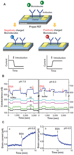
Figure 2 Electrical double layer in field-effect transistors (FETs).
Notes: (A) Schematic illustration of electrical double layer in a solution. Positive charges are accumulated near a channel. (B) Transfer characteristics in the graphene field-effect transistor against back gate voltage in vacuum (red line) and electrolyte gate voltage in a solution (blue line).Citation15 (C) shows the enlarged view of (B). Reprinted from Sensors Actuators B: Chem. Vol 187.Maehashi K, Sofue Y, Okamoto S, et al. Selective ion sensors based on ionophore-modified graphene field-effect transistors. 2013;187:45–49. Copyright 2013, with permission from Elsevier.Citation15
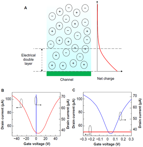
Figure 3 Electrical detection of biomolecules using buffer solution with low concentration.
Notes: (A) Multiplexed electrical detection of cancer markers with silicon (Si) nanowire (NW)-based sensor arrays. Prostate-specific antigen (PSA), carcinoembryonic antigen (CEA), and mucin-1 were monitored using three different Si nanowires, which were functionalized with antibodies for PSA, CEA, and mucin-1, respectively.Citation20 (B) Real-time electrical detections (upper right) of single virus using Si nanowire-based FETs. Optical images (lower right) using fluorescently labeled viruses supported the electrical measurements.Citation21 The red dots in the image show virus, and the solid and dashed white arrows correspond to the positions of the Si nanowire and a single virus, respectively.Citation21 Reprinted by permission from Macmillan Publishers Ltd: Nat Biotechnol. Zheng G, Patolsky F, Cui Y, et al. Multiplexed electrical detection of cancer markers with nanowire sensor arrays. 23:1294–1301, copyright 2005;Citation20 Reprinted by permission from Macmillan Publishers Ltd: Proc Natl Acad Sci USA. Patolsky F, Zheng G, Hayden O, et al. Electrical detection of single viruses. 101:14017–14022. Copyright (2004) National Academy of Sciences, U.S.A.Citation21
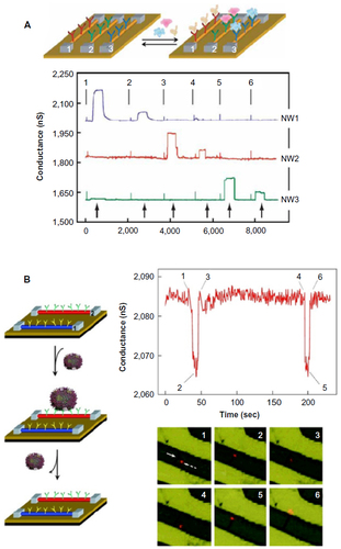
Figure 4 Electrical detection of biomolecules using small receptors.
Notes: (A) Real-time detection of immunoglobulin (Ig)E molecules in the range of 250 pM to 160 nM using aptamer-modified carbon nanotube (CNT) field-effect transistors (FETs) (left side). The adsorption of IgE on to aptamers on single-walled carbon nanotube channels follows the Langmuir adsorption isotherm (right side).Citation30 (B) Schematic illustration of an antibody and an antigen-binding fragment (Fab) (left side) and heat-shock protein concentration dependence of a drain current in an Fab-modified graphene FET (right side).Citation13 Reproduced with permission from Maehashi K and Matsumoto K. Label-free electrical detection using carbon nanotube-based biosensors. Sensors 2009;9:5368–5378. Copyright 2009 Multidisciplinary Digital Publishing Institute.Citation30 Reproduced with permission from Okamoto S, Ohno Y, Maehashi K, et al. Immunosensors based on graphene field-effect transistors fabricated using antigen-binding fragment. Jpn J Appl Phys. 2012;51:06FD08. Copyright 2012 The Japan Society of Applied Physics.Citation13
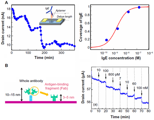
Figure 5 Silicon nanowire-based biosensors.
Notes: (A) Fabrication of silicon (Si) nanowire field-effect transistors (FETs) using bottom-up technology. The Si nanowires are grown using metal catalyst by vapor–liquid–solid method. Then, the Si nanowires are scattered on silicon dioxide (SiO2)/Si substrates. After formation of electrodes on the substrates, Si nanowire-based FETs can be fabricated.Citation47 (B) Fabrication of Si nanowire FETs using ultrathin Si on insulator substrates and anisotropic wet etching process.Citation36 Reprinted by permission from Macmillan Publishers Ltd: Nature Protoc. Patolsky F, Zheng G, Lieber CM. Fabrication of silicon nanowire devices for ultrasensitive, label-free, real-time detection of biological and chemical species. 1:1711–1724. Copyright 2006;Citation47 Reprinted by permission from Macmillan Publishers Ltd: Nature. Stern E, Klemic JF, Routenberg DA, et al. Label-free immunodetection with CMOS-compatible semiconducting nanowires.2007;445:519–522. Copyright 2007.Citation36
Abbreviations: S, source; D, drain; G, gate.
Abbreviations: S, source; D, drain; G, gate.
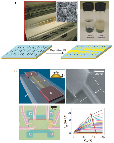
Figure 6 Carbon nanotube (CNT)-based biosensors.
Notes: (A) Position-controlled growth of single-walled carbon nanotubes (SWNTs) by patterned catalyst for fabrication of carbon nanotube field-effect transistors (FETs). First, a patterned catalyst is formed by photolithography and liftoff process on silicon (Si) substrates covered with a silicon dioxide (SiO2) layer. SWNTs are grown by chemical vapor deposition. Source and drain electrodes are fabricated on the patterned catalyst. Optical and scanning electron microscope (SEM) images of CNTFETs are shown. (B) Atomic force microscopy image of an SWNT network and schematic illustration of a network CNTFET.Citation56 (C) SEM image of horizontally aligned SWNTs between catalyst lines synthesized on quartz substrate and a schematic illustration of electrolyte-gated CNTFET sensor.Citation60 Reprinted with permission from Gui EL, Li L-J, Zhang K, et al. DNA sensing by field-effect transistors based on networks of carbon nanotubes. J Am Chem Soc. 129: 14427–14432. Copyright 2007 American Chemical Society.Citation56 Reprinted with permission from Okuda S, Okamoto S, Ohno Y, et al. Horizontally aligned carbon nanotubes on a quartz substrate for chemical and biological sensing. J Phys Chem C. 116:19490–19495. Copyright 2012 American Chemical Society.Citation60
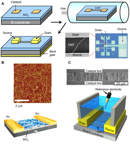
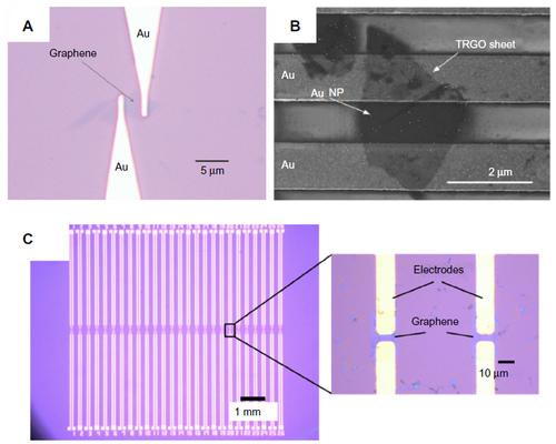
Figure 7 Graphene-based biosensors.
Notes: (A) Optical image of a graphene field-effect transistor (FET). The graphene was obtained by mechanical exfoliation.Citation37 (B) Scanning electron microscope image of a thermally reduced graphene oxide (TRGO) sheet with gold (Au) nanoparticle (NP)–antibody conjugates spanning across Au electrodes.Citation74 (C) Optical image of graphene–FET array. The graphene was synthesized by chemical vapor deposition.Citation84 Reprinted with permission from Ohno Y, Maehashi K, Yamashiro Y, et al. Electrolyte-gated graphene field-effect transistors for detecting ph and protein adsorption. Nano Lett. 9:3318–3322. Copyright 2009 American Chemical Society.Citation37 Reprinted from Mao S, Lu G, Yu K, et al. Specific protein detection using thermally reduced graphene oxide sheet decorated with gold nanoparticle-antibody conjugates. Adv Mater. 22:3521–3526. Copyright © 2010 WILEY-VCH Verlag GmbH & Co. KGaA, Winheim.Citation74 Reprinted from Zaifuddin NM, Okamoto S, Ikuta T, et al. pH sensor based on chemical-vapor-deposition-synthesized graphene transistor array. Jpn J Appl Phys. 52:06GK04. Copyright 2013 The Japan Society of Applied Physics.Citation84