
Abstract
This study investigated the charge injection and accumulation characteristics of organic light-emitting diodes (OLEDs) generated by spontaneous orientation polarization (SOP) of organic molecules. SOP enhances the electrical characteristics of OLED devices, such as charge injection and transport, by adjusting the interfacial charge density between the organic layers within the device. An OLED device with a mixed co-host emitting layer was fabricated to examine the degradation effect of SOP after electrical aging. Impedance spectroscopy (IS) revealed the presence of interfacial charges originating from the SOP of small molecules within the electron transport layer (ETL), in both pristine and aged devices. Furthermore, the IS simulation results using equivalent circuits were successfully interpreted based on the electrical properties of each organic layer in the pristine and aged devices. The electrical properties of the ETL, which contained 1,3,5-tris(N-phenyl benzimidazole-2-yl)benzene (TPBi), were degraded, reducing hole accumulation and electron injection.
1. Introduction
Organic light-emitting diodes (OLEDs) emit light from organic materials [Citation1]. OLED devices comprise various essential layers, including the hole injection layer (HIL), hole transport layer (HTL), emission layer (EML), electron transport layer (ETL), and electron injection layer (EIL). When a voltage is applied, holes and electrons are injected into the device through the anode and cathode, respectively. The injected charges overcome the energy barriers between the layers and reach the EML. Inside the EML, the transported hole–electron pairs form excitons, which emit light through the recombination of holes and electrons [Citation2]. The device structure is made more complex by incorporating various layers, such as hole-blocking and electron-blocking layers, to achieve stability and high efficiency in OLEDs and improve the charge balance between holes and electrons within the EML. However, the device structure can be simplified by constructing an EML using a co-host [Citation3,Citation4].
The EML of co-host EML OLEDs comprises different materials to achieve bipolar charge transport characteristics. Compared to single-host EML OLEDs, co-host EML OLEDs with a simplified structure can achieve a higher charge balance factor by incorporating hole transport and electron transport materials as the host material of the EML. Co-host EML OLEDs achieve high efficiency via efficient charge injection into the EML, superior charge balance, a wide recombination zone, and exciplex formation, contributing to the efficient emission of dopants [Citation3,Citation5].
According to Noguchi et al., controlling the accumulation characteristics of interfacial charges in OLEDs affects the electrical properties of these devices [Citation6,Citation7]. The injection and accumulation characteristics of charges are determined by factors such as energy barriers due to energy-level differences between each layer and the polarization of the materials [Citation8]. The transition dipole moment (TDM) possessed by the emitters in the EML exhibits variations in optical characteristics concerning the orientation angle of emitters. This can be investigated by measuring the optical property differences caused by changes in angle through Angular dependent Photoluminescence (ADPL) [Citation9]. On the other hand, the permanent dipole moment (PDM) held by charge transporting materials is crucial for charge injection and transport, necessitating an analysis of interfacial charge within the device. Organic molecules possess a PDM because of their characteristic anisotropic molecular structures and the moieties with various electronegativities. During thin-film deposition, the deposited organic layers exhibit spontaneous orientation polarization (SOP) when the organic molecules containing a PDM undergo orientational alignment [Citation8,Citation10]. Depending on the SOP polarity, a positive or negative interfacial charge (PIC or NIC) appears at the interface between the layers. An interfacial charge (IC) within a device creates an internal electric field that enables charge accumulation. Consequently, the electrical performance of OLED devices can be improved or diminished by manipulating the charge-accumulation characteristics associated with the SOP observed at the interface [Citation8,Citation11]. Therefore, analyzing SOP characteristics can enhance the efficiency and lifetime of OLEDs.
Examining the transport and accumulation of charge carriers is vital in improving OLED efficiency and device-driving stability [Citation12]. Impedance spectroscopy (IS) is commonly employed to study OLEDs based on current density–voltage-luminance (J-V-L) and electroluminescence characteristics [Citation13,Citation14]. IS effectively analyzes OLEDs by interpreting their behavior as a resistor–capacitor (RC) circuit, considering each organic layer’s inherent resistive and capacitive characteristics [Citation15]. The restricted charge flow characteristics under modulated AC voltage are identified using the impedance (Z), which exhibits a phase-shift factor between the AC voltage and the AC signal. The capacitance and resistance can be calculated using the real and imaginary components of the measured impedance spectra. By observing variations in capacitance values with respect to the measured DC voltage and frequency, a comprehensive analysis of charge-carrier dynamics, including injection, accumulation, and emission, can be achieved [Citation13].
In recent years, research has been conducted to control SOP and enhance OLED performance [Citation9,Citation16–22]. While most studies on SOP have focused on the characteristics of the ETL, only a few reports have addressed the significant impact of SOP on the lifetime of OLED devices [Citation23]. Moreover, few studies on the driving stability of OLED devices using IS have been initiated [Citation24–27].
In this study, co-host EML OLED devices composed of a blend of 1,3,5-tris(N-phenyl benzimidazole-2-yl)benzene (TPBi) and 4,4’,4''-tris(carbazol-9-yl)triphenylamine (TCTA) as host materials were analyzed, and each material exhibited either the presence or absence of SOP. Using IS, changes in charge carrier accumulation and transport were observed in both the pristine and aged co-host EML OLED devices. TPBi, which exhibits a strong NIC effect, facilitated hole accumulation at the HTL/EML interface of the pristine device. However, the degradation of TPBi hindered the accumulation of holes at the HTL/EML interface, resulting in an overall reduction in the current density and luminance of the co-host EML OLEDs.
2. Experimental
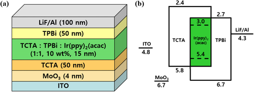
A glass substrate patterned with indium tin oxide (ITO), having a sheet resistance of 20 Ω/sq and a thickness of 150 nm, was employed. The bottom-emitting OLED comprised molybdenum trioxide (MoO3), TCTA (50 nm), EML (15 nm), TPBi (50 nm), and LiF/Al, as demonstrated in Figure (a). The EML was composed of a host material consisting of a 1:1 mixture of TCTA and TPBi, doped with 10 wt. % of the green phosphorescent dopant bis(2-phenylpyridine)(acetylacetonate)iridium(III) (Ir(ppy)2(acac)).
Figure 1. (a) Device structure of bottom emitting OLEDs, and (b) energy diagram of OLEDs.
The ITO-patterned glass substrates were cleaned with deionized water, acetone, and isopropyl alcohol and then dried in an oven at 150°C for 15 min. The organic layers and cathode were thermally evaporated in a high vacuum with a pressure below 10−6 torr. The fabricated OLEDs were then encapsulated in a nitrogen glove box.
All measurements were conducted at room temperature (RT). The measured J-V-L characteristics for the electrical analysis of the device were obtained using a Keithley 2400 instrument and a spectrometer (SpectraScan PR 650, Photo Research). The aged device, driven at 500 cd/m2 until the luminance reached 50% of that of the pristine device, was obtained using a lifetime tester (M600 PMX_4CH Lifetime Tester, McScience). Impedance analyses of both the pristine and aged devices were performed using an impedance analyzer (ModuLab XM MTS, Solartron Analytical) with an AC voltage of 80 mV over a frequency range of 10 Hz to 10 MHz. Z-view simulation software was used to simulate the mixed-host OLED. The capacitance and resistance were derived from Z’ and Z'’ when the organic semiconductor layer behaved like a dielectric material and was electrically equivalent to a parallel RC circuit.
3. Result and discussion
Figure (a and b) show the J-V-L and current density-efficiency characteristics, respectively. The pristine device exhibited a luminance turn-on of 2.8 V and a maximum current efficiency of 49.4 cd/A. Contrastingly, the aged co-host EML OLED device exhibited a luminance turn-on voltage of 3.4 V and a maximum current efficiency of 31.9 cd/A. The current density, luminance, and efficiency decreased after aging, indicating a deterioration in the electrical properties of the device. In Figure (a), the J-V turn-on voltage of the current density remains constant at 2.2 V for both the pristine device and aged devices. However, the luminance turn-on voltage increases from 2.8 V to 3.4 V. The J-V turn-on voltage indicates hole injection into the device, while the luminance turn-on voltage corresponds to the secondary charge injection of electrons and recombination between holes and electrons. The sequential charge injection can be attributed to the NIC effect, which enables hole injection before electron injection. The observed increase in luminance turn-on voltage compared to the pristine device suggests a delayed electron injection into the EML owing to device degradation. Further analysis based on the results of the IS analysis in Figure (a and b) will be discussed.
Figure 2. The electrical characteristics of the pristine and aged devices: (a) J-V-L characteristics, (b) current density-efficiency characteristics, and (c) normalized electroluminescence spectra of the OLEDs.
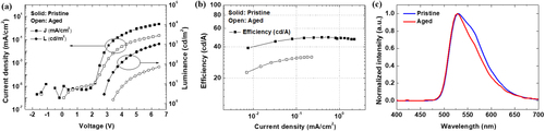
Figure 3. C-V and J-V-L characteristics for the (a) pristine device and (b) aged devices.
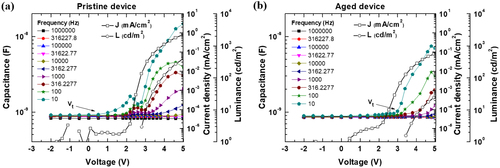
Figure (c) shows the normalized electroluminescence (EL) intensities of the devices. The EL spectrum can be red- or blue-shifted in OLEDs depending on the location of the recombination zone [Citation28–30]. The EL spectrum of the pristine device was relatively broad, exhibiting a shoulder peak at 550 nm compared with that of the aged device. A slight blue shift and the disappearance of the shoulder peak at 550 nm were observed in the EL spectrum of the aged device. The differences in the EL spectra of the two devices indicate that the recombination region shifted toward the ETL side in the aged device, owing to delayed electron injection after aging [Citation30]. The pristine device efficiently enhances charge injection, exhibiting a wide recombination zone covering the entire EML and a broad bandwidth of the EL spectrum. On the other hand, TPBi degradation in aged devices leads to an unbalanced charge injection into the EML. This causes the recombination zone to be biased toward the EML/ETL side, reducing the bandwidth of the EL spectrum.
The capacitance–voltage characteristics for varying frequencies in both the pristine (a) and aged devices (b) are illustrated in Figure . The pristine device exhibits the first peak at approximately 2 V and the second peak at approximately 4 V at 10 Hz, as depicted in Figure (a). The transition voltage (Vt) of the capacitance–voltage (C-V) curve occurs before the J-V turn-on voltage, as shown in Figure (a). Vt denotes the rising voltage of the C-V curve. The NIC effect generated by the SOP of TPBi enables hole injection, diffusion, and accumulation at the HTL/EML interface, increasing the capacitance of the devices [Citation31,Citation32]. The first peak of the C-V curve is formed by the transport and accumulation of holes at the HTL/EML interface when sufficient voltage is applied over Vt [Citation33]. Subsequently, the capacitance of the second peak increases, owing to various charge-trapping mechanisms of holes and electrons by the dopants in the EML. The recombination and nonradiative decay processes of excitons in the EML lead to reduced capacitance, thereby forming the second peak in the C-V curve.
A notable aspect of the C-V characteristics of the pristine and aged devices is the variation in Vt. The Vt of the aged device increased to 2.8 V compared to that of the pristine device, which was 0.6 V [Citation21,Citation31]. This difference was attributed to the delayed hole injection resulting from the disappearance of the NIC effect of TPBi. During device operation, small molecules can be degraded by various factors, such as thermal decomposition, electrochemical decomposition, molecular migration, and morphological instability [Citation34–37]. Among the various organic molecules used in our device, aged TPBi can reduce the NIC effect. Lin et al. reported that continuous operation of OLEDs promotes molecular migration of TPBi, even at a low operating bias, owing to the small size of the TPBi molecules [Citation36]. Liu et al. also investigated the migration of TPBi-dopant molecules in different hosts with various molecular weights and dipole moments. The migration of the TPBi molecules was successfully analyzed using X-ray photoelectron spectroscopy (XPS) according to the type of EML host material [Citation37]. Based on these previous analyses, we can conclude that the higher Vt of the aged device compared to that of the pristine device can be attributed to the rearrangement of the TPBi molecule, owing to continuous electrical stress. The NIC is formed by uncompensated PDMs of aligned molecules during film evaporation [Citation7]. Therefore, the aged device loses its NIC effect because of the random rearrangement of the TPBi molecules during the aging process.
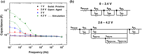
Figure (a) presents the capacitance-frequency (C-F) characteristics of the pristine and aged devices. The capacitance at high frequencies (104 Hz–105 Hz) corresponded to the geometric capacitance of the device. In the lower frequency range (101–103 Hz), the capacitance corresponded to the layers within the device, with plateaus depicting both accumulated and trapped charges within the device. Figure (a) displays a good agreement between the measurement and simulation results based on the equivalent circuit. Figure (b) indicates the equivalent circuit of the co-host EML OLED used in the C-F simulation. One organic layer corresponds to a parallel R-C component, and serially connected R-C circuits represent stacked organic layers. The equivalent circuit of 0–2.4 V represents the co-host EML OLED before charge injection into the EML. The equivalent circuit of 2.6 V–4.2 V represents the inclusion of trapping components for electrons and holes generated within the EML.
Figure 4. (a) C-F characteristics of the pristine and aged devices with simulation results and (b) equivalent circuits of the co-host EML OLEDs.
The relaxation frequency is the inverse of the time constant (τ), which is the product of the resistance (R) and capacitance (C) and represents the inflection point of the C-F curve. For example, the EML, with its large R, owing to the deep trap energy- level of dopant molecules and high C, owing to its thinner thickness compared to that of the HTL and ETL, has a large time constant and low relaxation frequency. Thus, the capacitance at each frequency region provides information about charge accumulation and trapping inside the OLED layers. Figure (a) reveals that the capacitance of the aged OLED was lower than that of the pristine OLED in the low-frequency region, suggesting that fewer charges were injected into the device during operation at the same voltage. To further elucidate the charge injection mechanism of the OLED, the R and C values of each layer were summarized and analyzed during the operating voltage, as specified in Figure .
Figure 5. Resistance-voltage-capacitance simulation results of the pristine and aged devices: (a) simulation results of the HTL and (b) ETL.
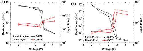
Figure demonstrates the resistance-voltage–capacitance simulation results for the HTL and ETL layers. The solid and open symbols represent the simulated values from the pristine and aged devices, respectively. In the voltage range of 0 V–2 V, the resistance of the HTL was lower than that of the ETL because of the pre-diffused holes injected by the NIC and faster hole mobility of TCTA (μh = 3.0 × 10⁻³ cm2/Vs) compared to the electron mobility of TPBi (μe = 3.3 × 10⁻⁵ cm2/Vs) [Citation38]. After reaching 2 V, a significant decrease in resistance was observed, which can be attributed to the increased hole and electron densities in the device after reaching the J-V turn-on voltage, as given in Figure . In contrast, the increasing capacitance observed in the same voltage region indicates the trapping of injected charges in the HTL and ETL. In Figure (b), as the voltage increases after 2 V, the resistance of the ETL decreases to 808 Ω because of the injection of electrons, while the capacitance increases to 2.4 × 10⁻⁸ F. The resistance drop voltage in Figure (a) is similar for the pristine and aged OLEDs because the J-V turn-on voltages of both devices were nearly identical, as depicted in Figure . However, the resistance drop voltage of the ETL in Figure (b) was significantly delayed because of the increase in the luminance turn-on voltage in the aged device, as previously observed in Figure . This indicates that the IS analysis reconfirmed that electron injection was hindered by the decreased NIC effect. The capacitance of the ETL was similar in all voltage ranges for the pristine and aged devices, implying that the degradation of TPBi was not caused by the formation of additional trap states, owing to the destruction of molecules.
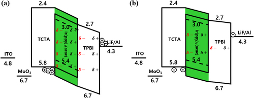
Figure illustrates the energy diagram of the pristine and aged devices, showing the internal charge transport in the Vt < V < Vbi voltage region. An interfacial charge was formed at the organic heterointerface, owing to the SOP properties of TPBi molecules [Citation25]. TPBi is a polar molecule, with a permanent dipole moment of 2.0 D. It exhibits negative interfacial charge (NIC) characteristics, showing δ- polarities toward anodes and δ+ polarities toward cathodes [Citation31,Citation38–40]. The NIC is generated by the SOP, promoting hole injection from Vt at a voltage lower than Vbi. Consequently, the accumulation of holes at the HTL/EML interface was observed before the J-V turn-on [Citation39,Citation41]. The different NIC effects of the EML and ETL can be attributed to the co-evaporated film of polar and non-polar molecules in the EML. The co-evaporated film forms a larger electric field than that of a neat film composed only of polar molecules, owing to the decreased interaction between the PDM of the polar molecules [Citation27,Citation42]. In Figure (b), the NIC decreases after the aging of the device, as explained by the C-V characteristics in Figure . Based on the previous analysis, we concluded that the randomly rearranged TPBi molecules decreased the SOP of the EML and ETL in the aged device and weakened the NIC effect. Consequently, charge injection and current efficiency were reduced in the aged device owing to the weakened NIC effect caused by TPBi degradation.
Figure 6. Energy diagram in Vt < V < Vbi region of the (a) pristine and (b) aged devices.
4. Conclusion
In summary, degradation of the charge injection and accumulation characteristics at the organic interface, originating from SOP, were observed between the pristine and aged devices of the co-host EML OLEDs. The J-V-L and C-V characteristic analyses reveal that the NIC-induced hole injection occurred before the J-V turn-on voltage, leading to accumulated holes at the HTL/EML interface and enhanced electron injection. The overall decrease in the electrical properties of the aged co-host EML OLEDs, along with the degradation, was attributed to TPBi degradation. Furthermore, we expect that the impedance spectroscopy analysis of aged OLEDs, based on the NIC and SOP of organic molecules, will help elucidate the stability mechanisms of OLED devices.
Acknowledgments
This work was supported by the Technology Innovation Program (20020408, Development of direct analytic methods for exciton dynamics in OLEDs and lifetime-enhancing technologies based thereon) funded by the Ministry of Trade, Industry & Energy (MOTIE, Korea).
Disclosure statement
No potential conflict of interest was reported by the author(s).
Additional information
Notes on contributors

So-Young Boo
So-Young Boo received her B.S. degree from Hanbat National University, South Korea, in 2022. She is currently taking the M. S. course at the same university. Her research is focused on the organic semiconductor, charge dynamics, and impedance spectroscopy.

Akeem Raji
Akeem Raji received his BSc. degree in Materials Engineering from Kwame Nkrumah University of Science and Technology, Kumasi, Ghana, in 2018. He furthered his education in South Korea, where he obtained his Master of Engineering degree (MEng) from Hanbat National University. He is currently a Ph.D. student. His research is focused on organic semiconductors and nanofabrication of thin film.

Jae-Yong Park
Jae-Yong Park is taking an M.S. course in the Department of Creative Convergence Engineering at Hanbat National University. His research interests include impedance analysis.

Somi Park
Somi Park received her B.S. degree from Hanbat National University, South Korea, in 2023. She is currently taking the M.S. course in the Department of Creative Convergence Engineering at Hanbat National University. Her research interests include doped organic semiconductors.

Jonghee Lee
Jonghee Lee received his B.S., M.S., and Ph.D. in Chemistry from the Korea Advanced Institute of Science and Technology (KAIST) in 2002, 2004, and 2007, respectively. He joined the Electronics Telecommunications Research Institute (ETRI) in Korea in 2007. Then, he moved to the Institut für Angewandte Photophysik (IAPP) at the Technische Universität Dresden in Germany as a post-doc researcher under an Alexander von Humboldt fellowship in 2010. After two years, he rejoined ETRI and has worked on solution processes and light-extraction techniques for organic light-emitting diodes (OLEDs). He has been an associate professor at Hanbat National University, Daejeon, South Korea, since 2018.

Jae-Hyun Lee
Jae-Hyun Lee is a professor in the Department of Creative Convergence Engineering at Hanbat National University. He received his B.S. and Ph.D. degrees from the Department of Materials Science and Engineering at Korea University in 2002 and Seoul National University in 2011, respectively. Then he worked as a post-doctoral fellow at Institut für Angewandte Photophysik (IAPP) at Technische Universität Dresden (TU Dresden). His research areas include flexible organic electronics and electrically doped organic semiconductors.
References
- B. Geffroy, P.L. Roy, and C. Prat, Polym. Int. 55, 572–582 (2006).
- S. Nowy, W. Ren, J.A. Weber, and W. Brütting, Proc. SPIE 7415, 74150G (2009).
- W. Song, and J.Y. Lee, Appl. Phys. Lett. 106, 123306 (2015).
- Q. Wang, Q. Tian, Y. Zhang, X. Tang, and L. Liao, J. Mater. Chem. C 7, 11329–11360 (2019).
- J. Lee, P. Choi, M. Kim, K. Lim, Y. Hyeon, S. Kim, K. Koo, S. Kim, and B. Choi, J. Nanosci. Nanotechnol. 18, 5908–5912 (2018).
- Y. Noguchi, A. Hofmann, and W. Brütting, Adv, Optical Mater. 10, 2201278 (2022).
- L. Jäger, T.D. Schmidt, and W. Brütting, AIP Adv. 6, 095220 (2016).
- Y. Noguchi, Y. Tanaka, H. Ishii, and W. Brütting, Synth, Met. 288, 117101 (2022).
- A. Hofmann, M. Schmid, and W. Brütting, Adv, Optical Mater. 9, 2101004 (2021).
- K. Osada, K. Goushi, H. Kaji, C. Adachi, H. Ishii, and Y. Noguchi, Org. Electron. 58, 313–317 (2018).
- Y. Noguchi, K. Ninomiya, and K. Sato, J. Phys. Chem. C 126, 18520–18527 (2022).
- B. Chin, J. Phys. D: Appl. Phys. 44, 115103 (2011).
- A. Gasonoo, Y. Lim, E. Jang, J. Lee, M. Kim, Y. Choi, and J. Lee, Mater. Today Energy 21, 100794 (2021).
- H. Choi, S. Lee, Y. Lim, S. Lee, J. Lee, and J. Lee, AIP Adv. 10, 065226 (2020).
- V. Bender, N.D. Barth, F.B. Mendes, R.A. Pinto, T. Marchesan, and J.M.A. Alvarez, IEEE Electron. Device Lett. 3, 1190–1195 (2015).
- P. Liehm, C. Murawski, M. Furno, B. Lüssem, K. Leo, and M.C. Gather, Appl. Phys. Lett. 101, 253304 (2012).
- Y. Noguchi, Y. Miyazaki, Y. Tanaka, N. Sato, Y. Nakayama, T.D. Schmidt, W. Brütting, and H. Ishii, J. Vac. Soc. Jpn. 58, 37 (2015).
- Y. Noguchi, K. Ninomiya, and K. Sato, J. Phys. Chem. C 126, 18520–18527 (2022).
- B.A. Naqvi, M. Schmid, E. Crovini, P. Sahay, T. Naujoks, F. Rodella, Z. Zhang, P. Strohriegl, S. Bräse, E.Z. Colman, and W. Brütting, Front. Chem. 8, 750 (2020).
- Y. Noguchi, K. Osada, K. Ninomiya, H.D.C.N. Gunawardana, K.R. Koswattage, and H. Ishii, J. Soc. Inf. Disp. 29, 29–37 (2021).
- S. Sato, M. Takada, D. Kawate, M. Takata, T. Kobayashi, and H. Naito, Jpn. J. Appl. Phys. 58, SFFA02 (2019).
- K. Osada, K. Goushi, H. Kaji, C. Adachi, H. Ishii, and Y. Noguchi, Org. Electron. 58, 313–317 (2018).
- Y. Noguchi, W. Brütting, and H. Ishii, Jpn. J. Appl. Phys. 58, SF0801 (2019).
- J. Wang, X. Zhang, L. Fan, X. Zhang, Y. Qin, R. Li, Y. Chen, W. Lai, X. Zhang, and W. Huang, J. Mater. Chem. C 8, 9909–9915 (2020).
- V. Jankus, C. Chiang, F. Dias, and A.P. Monkman, Adv. Mater. 25, 1455–1459 (2013).
- B. Kim, and J. Lee, Adv. Funct. Mater. 24, 3970–3977 (2014).
- C.K. Vipin, A. Shukla, K. Rajeev, M. Hasan, S.C. Lo, E.B. Namdas, A. Ajayaghosh, and K.N. Narayanan Unni, J. Phys. Chem. C 125, 22809 (2021).
- C.-H. Hsiao, Y. Chen, T. Lin, C.C.-C. Hsiao, and J. Lee, Appl. Phys. Lett. 89, 163511 (2006).
- G. Huseynova, J.-H. Lee, A. Gasonoo, H. Lee, Y.H. Kim, and J. Lee, J. Inf. Disp. 23, 259–266 (2022).
- W. Lee, D. Kim, P.J. Jesuraj, H. Hafeez, J. Lee, D. Choi, T. Bae, S. Yu, M. Song, C. Kim, and S. Ryu, Mater. Res. Express. 5, 076201 (2018).
- Y. Noguchi, H. Kim, R. Ishino, K. Goushi, C. Adachi, Y. Nakayama, and H. Ishii, Org, Electron. 17, 184–191 (2015).
- K. Davenport, T.K. Djidjou, S. Li, and A. Rogachev, Org, Electron. 46, 166–172 (2017).
- L. Zhang, H. Nakanotani, and C. Adachi, Appl. Phys. Lett. 103, 093301 (2013).
- H. Aziz, and A.D. Popovic, Chem. Mater. 16, 4522–4532 (2004).
- J. Jou, Y. Lin, Y. Su, W. Song, S. Kumar, D.K. Dubey, J. Shyue, H. Chang, Y. You, and T. Liang, Org. Electron. 67, 222–231 (2019).
- W. Lin, W. Wang, Y. Lin, B. Yu, Y. Chen, M. Hsu, J. Jou, and J. Shyue, Org. Electron. 10, 581–586 (2009).
- C. Liu, W. Wang, C. Lin, W. Lin, C. Liu, C. Kuo, S. Lee, W. Kao, G. Yen, Y. You, and H. Chang, J. Jou. J. Shyue. Org. Electron. 12, 376–382 (2011).
- S.-J. Kim, A. Raji, A. Gasonoo, J. Lee, and J.-H. Lee, Org. Electron. 120, 106850 (2023).
- W. Brütting, S. Berleb, and A.G. Mückl, Org. Electron. 2, 1–36 (2001).
- Y. Noguchi, Y. Miyazaki, Y. Tanaka, N. Sato, Y. Nakayama, T.D. Schmidt, W. Brütting, and H. Ishii, J. Appl. Phys. 111, 114508 (2012).
- S. Berleb, W. Brütting, and G. Passch, Org. Electron. 1, 41–47 (2000).
- Y. Noguchi, N. Sato, Y. Miyazaki, Y. Nakayama, and H. Ishii, Jpn. J. Appl. Phys. 49, 01AA01 (2010).