Figures & data
Figure 1. The schematic of the structure of TQLEDs.
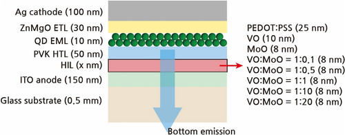
Figure 2. XPS peak analysis of (a) V 2p5/2 peak and (b) O 1s peak of VO:MoO = 1:1 film, (c) Mo 3d5/2 peak of MoO film, and (d) peak ratio variations according to MoO mixing ratio. Peaks in Figure (a–c) were deconvoluted using Gaussian functions.
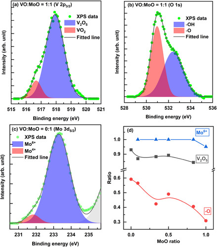
Figure 3. (a) Secondary electron cutoff and (b) HOMO regions of the UPS spectra of HILs, (c) bandgap energy of VO:MoO HILs according to the MoO mixing ratio, and (d) energy bands of HILs and PVK HTL. A fixed vacuum level for all layers was used for this diagram. The green dotted line indicates the HOMO level of the VO:MoO = 1:1 HIL.
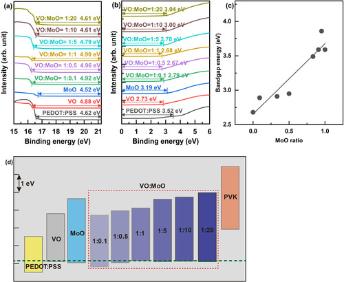
Figure 4. (a) Current density – bias voltage curves of hole-dominant devices according to the MoO mixing ratio in VO:MoO HIL materials and (b) schematic illustrating the device structure of the hole-dominant devices.
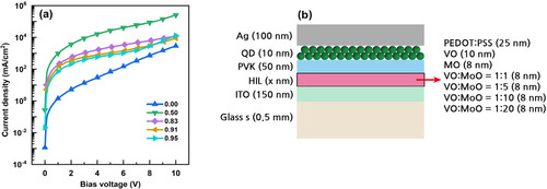
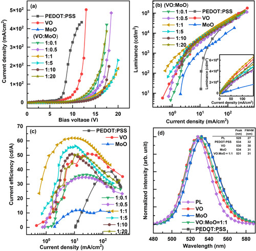
Figure 5. (a) Current density – bias voltage curves, (b) luminance – current density curves, and (c) current efficiency – current density curves of QLEDs according to the HIL materials. (d) PL and EL spectra of QLEDs. The HIL materials of the QLEDs are indicated in the figure legends. Luminance – current density curves in linear scale are shown as an inset in Figure (c), and the table showing peak wavelength and FWHM values is represented as an inset in Figure (d).