Figures & data
Figure 1. POM images for TESADT films annealed at T=(a) 100°C, (b) 105°C, (c) 110°C, (d) 115°C and (e) 120°C for 2 min. The white scale bar in panels (a–d) indicates 100 μm and (e) indicates 1 mm. The post-anneal crystalline domain size decreases for T>100°C with amorphous films obtained for T>115°C.
Figure 2. A POM study of domain size versus thermal anneal temperature T (horizontal axis) and time t (vertical axis) for T<100°C. The white scale bars indicate 1 mm. The optimal anneal conditions are T∼ 90°C for t∼ 3 min.
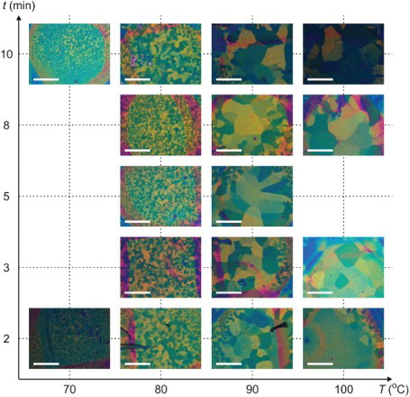
Figure 3. POM images of the best outcomes obtained using optimised (a) thermal- and (b) solvent-annealing processes. The images are composites of 25 smaller overlapping fields to enable the entire 10×10 mm area of the chip to be imaged (n.b., the tile-like contrast changes are an artefact). The white scale bars indicate 2 mm. (c–f) POM sequence showing the effect of alternating thermal (T) and solvent (S) anneals. The sequence begins with a solvent-annealed film (c), the remaining images are obtained after (d) a 2 min thermal anneal at 95°C, (e) a 2 min solvent anneal in dichloroethane vapour and (f) a second 2 min thermal anneal at 95°C. No visible change in the crystalline domain structure is obtained after the initial anneal confirming that both anneals drive towards the same crystal structure.
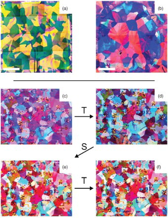
Figure 4. The drain current Id versus drain voltage Vd for gate voltages from Vg=−50 V (top) to 0 V (bottom) in steps of 10 V for spin-coated TESADT transistors crystallised using (a) a 2 min solvent anneal in dichloroethane vapour, and (b) a 5 min thermal anneal at 90°C, and for (c and d) drop-cast TESADT transistors crystallised using (c) a 2 min solvent anneal in dichloroethane vapour, and (d) a 5 min thermal anneal at 90°C.
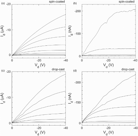
Figure 5. The drain current Id versus gate voltage Vg for drain voltage Vd=−30 V for each of the four different TESADT transistors in . The lines are measured transfer characteristics. The data points are extracted directly from to demonstrate correspondence between the transfer and source–drain characteristics for the four devices.
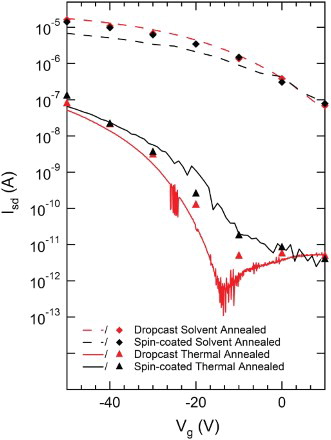
Table 1. Key electrical performance parameters for the four types of TESADT thin-film transistors studied.
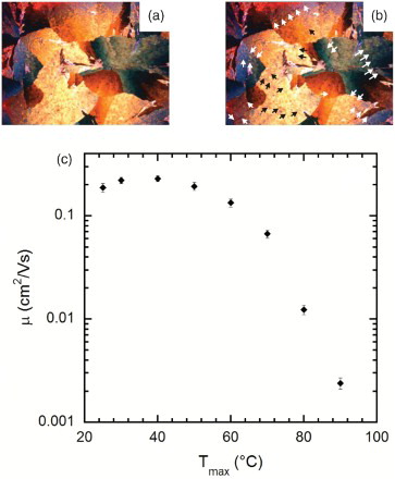
Figure 6. POM images (a) before and (b) after thermal annealing of a solvent-annealed TESADT film. The black and white arrows in (b) indicate cracks that developed during thermal annealing. (c) The field-effect mobility μ versus maximum anneal temperature for a TESADT transistor that underwent subsequent 2 min thermal anneals at T=30, 40, 50, 60, 70, 80 and 90°C, with electrical measurements performed at 25°C between each anneal. The initial point at T=25°C indicates a sample measured prior to any thermal annealing.