Figures & data
Figure 1. Description of the etching process of the BDD film based on the use of a hybrid organic/mineral photoresist mask.
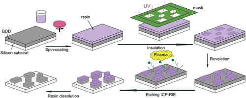
Figure 2. SEM image of a BDD film etched at 10 mTorr with a ratio Ar/O2=5/40 (sccm/sccm) and a RF power 100 W.
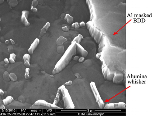
Figure 3. SEM images of a BDD film etched at 10 mTorr and 100 W with (a) Ar=11% vol. (ratio Ar/O2=5/40), (b) Ar=27% vol. (ratio Ar/O2=15/40) and (c) Ar=43% vol. (ratio Ar/O2=30/40 (sccm/sccm)).
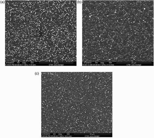
Figure 4. Effect of Ar content on the etch rate of the BDD film. O2 flux 40 sccm, RF power 100 W, pressure 10 mTorr, and etching time 10 min.
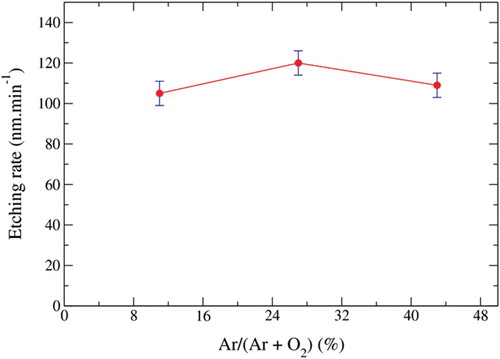
Figure 5. Effect of the RF power on the etch rate of the BDD film. Ar/O2=15/40 (sccm/sccm), pressure 10 mTorr and etching time 10 min.
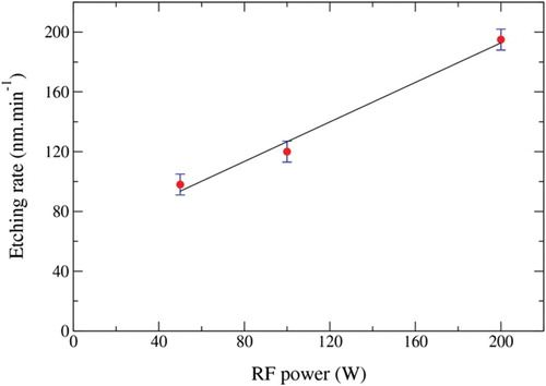
Figure 6. SEM images of the etched film with Ar/O2 15/40 (sccm/sccm), pressure 10 mTorr, etching time 10 min and RF power 100 W (a) and 200 W (b).
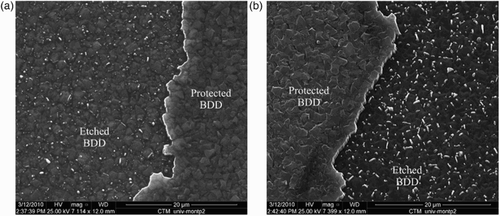
Figure 7. Effect of the pressure on the etching rate of BDD film (Ar/O2 15/40 (sccm/sccm), etching time 10 min and an RF power 100 W).
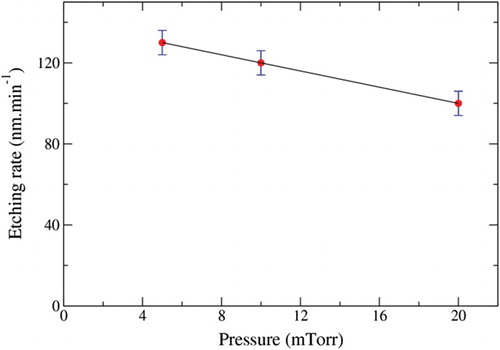
Figure 8. SEM image of the etched film with CHF3/O2 5/40 (sccm/sccm), pressure 10 mTorr, etching time 10 min and an RF power 200 W.
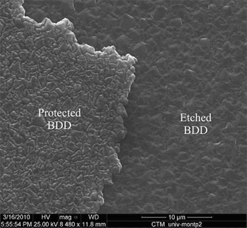
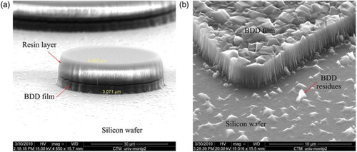
Figure 9. SEM images of different areas of the BDD film etched under a flux of Ar/O2 15/40 (sccm/sccm), at 10 mTorr with an RF power of 200 W (a) before and (b) after resin dissolution. The thicknesses of the BDD film and of the resin layer are 3.6 and 8.5 μm, respectively.