
Figures & data
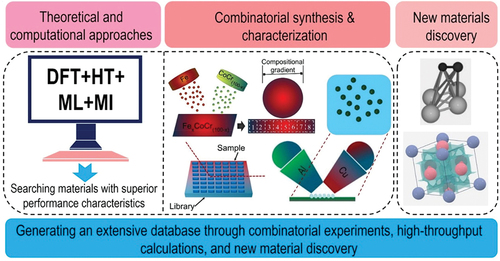
Figure 1. Illustration of the general process of high throughput material synthesis and characterization, which involves combining theoretical material theory, modeling, and material database development. The diagram shows that this process typically involves multiple stages, such as design and synthesis, characterization, and data analysis.
Figure 2. Illustrates two different approaches to high throughput material synthesis and screening. A combinatorial thin film material synthesis method is shown, where the thin film fabrication process is integrated in parallel using spatially addressable arrays of samples. A high throughput semiconductor thin film material screening process is depicted on the left side. Adapted from reference with permission [Citation47]. Copyright © 2015 The Chinese Ceramic Society.
![Figure 2. Illustrates two different approaches to high throughput material synthesis and screening. A combinatorial thin film material synthesis method is shown, where the thin film fabrication process is integrated in parallel using spatially addressable arrays of samples. A high throughput semiconductor thin film material screening process is depicted on the left side. Adapted from reference with permission [Citation47]. Copyright © 2015 The Chinese Ceramic Society.](/cms/asset/37ddd4b5-f076-4d0b-8b6d-47cd565153da/tstm_a_2292486_f0002_oc.jpg)
Figure 3. (a) Controlling formation of conductive filaments in hf-ta anodic oxides: a significant accomplishment in resistive random-access memories (b) revolutionizing flexible electronics: high throughput synthesis and anodic printing process, reproduced with permission [Citation49].
![Figure 3. (a) Controlling formation of conductive filaments in hf-ta anodic oxides: a significant accomplishment in resistive random-access memories (b) revolutionizing flexible electronics: high throughput synthesis and anodic printing process, reproduced with permission [Citation49].](/cms/asset/29b00040-d0f2-4154-9c9b-579c6b3a71f4/tstm_a_2292486_f0003_b.gif)
Figure 4. The elemental distribution of Ni, Ti, Cu, and V on a si wafer, with each element’s composition indicated by a color scale ranging from high (yellow) to low (green) atomic percentage.
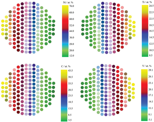
Figure 5. An illustration of a SnO2 film on a polycrystalline CoNb2O6 substrate, where each grain of the substrate allows the growth of SnO2 with a unique orientation relationship. The film consists of two types of SnO2: stable rutile (r-) SnO2 on some grains, and metastable scrutinyite-structured SnO2 on others.
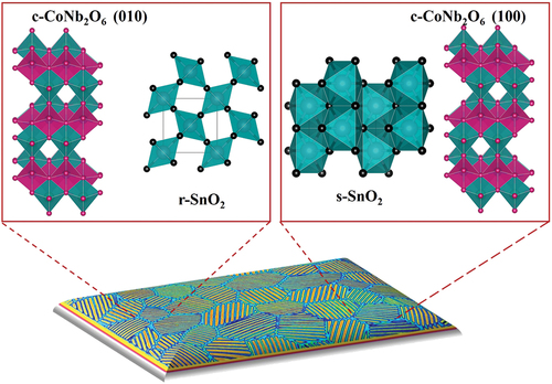
Figure 6. Illustration of high throughput material characterization which shows a schematic of high throughput composition and microstructure characterization using micro-beam X-ray fluorescence and diffraction. High throughput band-gap characterization based on optical transmission and transport property characterization based on ultrafast pulsed laser excitation can also be seen.
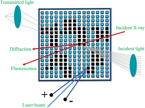
Figure 7. The left image illustrates the integrative role of data science, while the right image highlights the five defining characteristics of BigData.
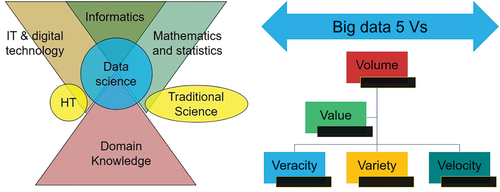
Table 1. Compilation of software’s for conducting electronic structure calculations in the field of computational materials science.
Table 2. A comprehensive toolkit for high-throughput simulation results generation, manipulation, management, and analysis.
Table 3. Compilation of libraries and platforms for machine learning and materials prediction.
Figure 8. A visual representation depicting the application of machine learning in materials science. Modified with permission from reference [Citation214].
![Figure 8. A visual representation depicting the application of machine learning in materials science. Modified with permission from reference [Citation214].](/cms/asset/a3907606-8cd0-4b65-a146-da0dda4643ee/tstm_a_2292486_f0008_oc.jpg)
Figure 9. Feedback derived from the experiments included the augmentation of the dataset with the addition of four newly discovered alloys. Modified with permission from reference [Citation216].
![Figure 9. Feedback derived from the experiments included the augmentation of the dataset with the addition of four newly discovered alloys. Modified with permission from reference [Citation216].](/cms/asset/be8c2204-69b9-4091-941b-89fa2208ed3c/tstm_a_2292486_f0009_oc.jpg)
Figure 10. Materials informatics workflow depicting the progression through traditional paradigms to the fourth paradigm shift.
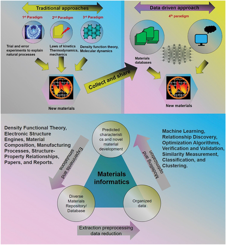
Figure 11. Materials informatics and the workflow involving machine learning for mechanical deformation strategy. Adopted with permission [Citation229].
![Figure 11. Materials informatics and the workflow involving machine learning for mechanical deformation strategy. Adopted with permission [Citation229].](/cms/asset/bdf6f7c1-79bd-47f5-91b2-971d2c6161c7/tstm_a_2292486_f0011_oc.jpg)
Figure 12. Illustration of the computational material design process, which involves investigating a large number of compounds to identify stable materials.
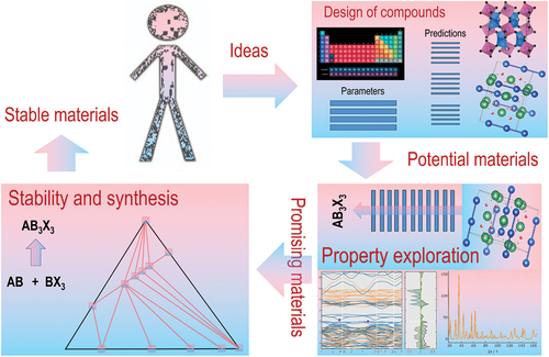
Figure 13. The collaborative approach of combining combinatorial synthesis, high-throughput calculations, and data sciences in the development of new materials for lithium batteries.
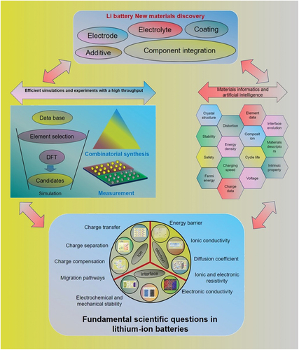
Figure 14. The evolving trajectory of lithium batteries in the near future, incorporating high-throughput simulations, high-throughput experiments, data mining, and artificial intelligence.
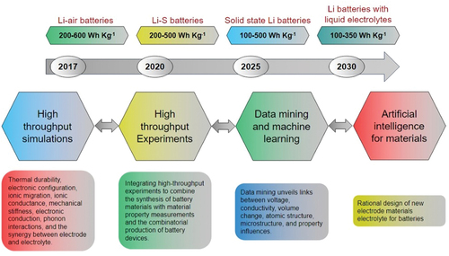
Figure 15. The Ada self-driving laboratory. Adopted with permission from reference [Citation295].
![Figure 15. The Ada self-driving laboratory. Adopted with permission from reference [Citation295].](/cms/asset/a717d963-060d-4df7-8808-68c6eb99430b/tstm_a_2292486_f0015_oc.jpg)