
Abstract
The detection of molecules dissolved in liquid medium can be envisaged by means of an optical integrated sensor operating in middle infrared range. The intended sensor is composed of a cladding and a guiding selenide sputtered layers transparent in middle infrared. Hence, Ge-Sb-Se thin films were selected in view of tailored refractive index contrast, successfully deposited by radio frequency magnetron sputtering and characterized. To maximize the evanescent field at a wavelength of 7.7 µm, a suitable selenide waveguide allowing measuring the optical transmitted power was designed by performing computer simulations based on the effective index method enabling single-mode propagation for a waveguide width between 8 and 12 µm. Selenide sputtered films were micro-patterned using reactive ion etching with inductively coupled plasma process. Finally, optical waveguide surface was functionalized by the deposition of a hydrophobic polymer, which will permit detection of organic molecules in water.
Introduction
The development of sensor enabling in situ detection of organic molecules in water by means of optical method is a vast ecological challenge [Citation1,2]. The chemical molecules that spread in the water lead to high monitoring requirements: high stability, sensitivity, multiplexing opportunities, large sensing range, compactness and short response time. Due to the absorption phenomenon in the middle-infrared (mid-IR) range (2·5–25 μm) caused by the fundamental vibrational transitions of organic molecules, this spectral range turned into a key choice within bio-chemical sensing in the gas or liquid state [Citation3–5]. Accordingly, the analysis of food, drinks, toxic agents, explosives, greenhouse gases, air and water pollutants, pharmaceutical systems, proteins, cells and polymers is naturally performed by mid-IR spectroscopy which is frequently used in Chemistry, Manufacturing and Control process. The potential of mid-IR photonics implementation is considerable including the (bio)-chemical sensors for environmental monitoring, security, and medical diagnostics. Among the various categories of optical sensor including the conventional attenuated total reflectance (ATR), the detection by means of evanescent field is one of the possible ways to allow the miniaturization of the sensor device with integration of mid-infrared photonic components and low-cost production [Citation6]. The evanescent field, i.e. a fraction of the guided light outside of the waveguide, can probe the external medium surrounding the waveguide sensitive to the optical changes induced by the analyte, such as its absorption. For mid-IR spectroscopy, quantum-cascade lasers are standard sources since their emission wavelength goes from the mid-IR to the far-IR with high power efficiency [Citation7]. Concerning, the optical platform -the key-stone of the sensor-, while other mid-IR platforms have been investigated lately, such as germanium (Ge) [Citation8] and gallium arsenide (GaAs) [Citation9], chalcogenide glasses has attracted attention for sensing applications due to their wide transparency in the infrared range [Citation1,14], their ability to be fabricated in thin film by PVD and manufactured into integrated photonic components by photolithographic and etching process. Current works have reported the mid-IR loss propagation [Citation10,11] and high quality factor micro-cavities [Citation6,12,13] of integrated chalcogenide devices. Additionally, organic substances have been detected using chalcogenide films, ethanol dissolved in cyclohexane [Citation6] at λ = 5·2 μm and anti-Salmonella – anti-E. coli, protein like avidin [Citation14,15] and 4-nitrothiophenol [Citation16] using a FTIR in reflexion or transmission mode.
In this article, we report the development of chalcogenide mid-IR platform devoted to mid-IR spectroscopy by means of evanescent wave. The choice of chalcogenide glass composition, the chalcogenide films synthesis through RF magnetron sputtering, the theoretical approach for defining the analytical design of the evanescent optical field sensor for detection of pollutants in water, the patterning of the films by means of photolithography and reactive ion etching, the optical losses and the surface functionalization of the sensor will be described.
Experimental methods
The mid-IR waveguide is composed of two layers (on silicon substrate), transparent in mid-IR presenting refractive index contrast; the first layer deposited on silicon substrate is a Ge–Sb–Se selenide film corresponding to the cladding layer and the second layer – the guiding layer – is a similar selenide film with different proportion of chemical elements in order to increase the refractive index in mid-IR [Citation17]. Consequently, Ge28.1Sb6.3Se65.6 and Ge12.5Sb25Se62.5 selenide glasses were synthetized and used as targets for thin films deposition by means of RF magnetron sputtering [Citation18]. The fabrication of thin films was carried out under Ar pressure of about 1·10−2 mbar and low RF working power; 20 W for Ge28.1Sb6.3Se65.6 and 10 W for Ge12.5Sb25Se62.5 targets. The morphology and chemical composition of targets, films and mid-IR structures were measured using a scanning electron microscope (SEM) with an energy-dispersive X-ray analyzer (EDS, JSM 6400-OXFORD Link INCA). Roughness of thin films was studied by atomic force microscopy (AFM, Ntegra Prima, NT-MDT). Tapping mode imaging was used on 2 μm × 2 μm area. Linear refractive indices of glasses, thin films and each layer of mid-IR guiding structure were obtained from the analysis of variable angle spectroscopic ellipsometry (VASE) data measured using two ellipsometers in UV-vis-NIR (300–2300 nm) and in NIR-MIR (1·7–30 μm) (J.A. Woollam Co., Inc., Lincoln, NE, U.S.A.).
Simulations to determine the design of optical waveguide working in mid-IR (at 7·7 μm) were performed based on refractive index contrast determined by VASE [Citation17,19,20]. The thicknesses (h) of both chalcogenide layers and the width (w) of the waveguide were established using a commercial software (FIMMWAVE, Photon Design) in order to obtain single-mode propagation at 7·7 μm and to maximize evanescent power factor ƞ in the superstrate [Citation21,22]. A 5 μm-thick Ge28.1Sb6.3Se65.6 confinement layer was found to be sufficient to avoid radiation losses through the substrate. Thickness of Ge12.5Sb25Se62.5 guiding layer between 1·5 and 2 μm allows obtaining single-mode propagation at a wavelength of 7·7 μm for a waveguide width between 8 and 12 μm and TM polarization. An optimal evanescent power factor of 5% was obtained for a 10 × 1·7 μm2 ridge waveguide (width × height), this calculation is based in the Effective Index Method. Then, ridge waveguides of different widths were fabricated using a classical i-line photolithographic process (MJB4 Suss Microtech mask aligner) followed by a dry etching procedure at low pressure combining reactive ion etching (RIE) and inductively coupled plasma (ICP) etching [Citation18,19]. Optical characterizations were performed by coupling a QCL emitting at 7·7 μm (1290 cm−1) from Alpes Lasers into the ridge waveguides through a ZnSe microscope objective (Innovation Photonics) and imaging the output facet on a microbolometer-based focal plane array (FPA, Optris PI400) using a second ZnSe microscope objective.
Optical loss measurement was executed using surface imaging method within the IR guiding structure [Citation19].
Results and discussion
Ge–Sb–Se targets and films characterization
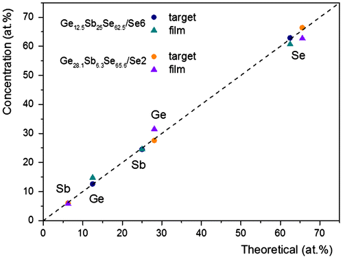
In the ternary Ge–Sb–Se system, pseudo-binary (GeSe2)100−x(Sb2Se3)x (x = 5, 10, 20, 30, 40, 50 and 60) glasses were studied for photonics applications concerning nonlinear optics or sensors. This system was preferred for its broader transmission window in infrared spectral region compared to sulfide glasses and films, high stability against crystallization with larger glass-forming system compared to telluride glasses and even films allowing tailoring of physical parameters of interest in broad ranges and lastly, suitable refractive index contrast. Moreover arsenic-containing compositions, toxic in its elemental form, could be unacceptable for end-users especially for continuous water analysis. Also, the presence of antimony in amorphous chalcogenides is known to reduce photosensitivity of both, the bulk glasses and thin films which can induce formation of oxide crystallites on layer surface as observed for As2Se3. Two nominal compositions, Ge28.1Sb6.3Se65.6 (x = 10) and Ge12.5Sb25Se62.5 (x = 50), were selected for this aim. The fabrication of these two distinct selenide films has been optimized by the experimental design approach in order to fully meet the criteria for producing optical components devoted to optical bio-chemical sensor applications, for which controlling the layer homogeneity is fundamental for thicknesses of few μm (from 1 to 6 μm). The chemical composition of Ge28.1Sb6.3Se65.6 and Ge12.5Sb25Se62.5 bulk targets and sputtered thin films is presented in Figures and . The chemical composition of chalcogenide targets is in good agreement with the theoretical composition and the Ge28.1Sb6.3Se65.6 and Ge12.5Sb25Se62.5 sputtered thin films deposited under 1·10−2 mbar Ar pressure are relatively close to the nominal composition of target with an excess in germanium, 3·9 and 2·2 at. % and a deficit can be noted, 3·7 and 2·2 at. % in the case of selenium. The difference between composition of the target and the thin films can be explained to a certain extent by a sputtering yield of each component of the complex Ge–Sb–Se targets. For comparison purposes, the sputtering yield values of single component targets around 1–1·5, 2·8–4·1 and 5·2–7·4 atom/ion for germanium, antimony and selenium targets, respectively, can be mentioned. These sputtering yields data represent the number of atoms ejected from the target per argon ion striking normally on the surface of the target with a classical kinetic energy range from 500 to 1000 eV. Nevertheless, magnetron design factors such as magnetic field strength, radio-frequency (13·56 MHz) and process parameters will affect the sputtering yields. For Ge–Sb–Se amorphous targets, other factors have to be considered such as the chemical bond energy of Ge–Se and Sb–Se bonds which predominate in the glass network, atomic weights of the three elements constituting the target, amorphous nature and density affecting a surface binding energy of the target atoms. Considering the higher sputtering yield of a chalcogen element in the single component target, it can be assumed that the Ge–Sb–Se target surface will quickly impoverish in Se, until an equilibrium composition is reached leading to deficiency in selenium at the surface of the target. Conversely, the surface layer of the target will be enriched with the element having the lower sputtering yield, i.e. germanium. Usually, during sputtering of a multicomponent target, the more volatile element is preferentially eliminated (i.e. selenium from Ge–Sb–Se target), so the surface of the sputtering target is enriched by less volatile constituents [Citation23]. That can amplify the higher sputtering yield of selenium compared to Ge and Sb in the Ge–Sb–Se multicomponent target. Indeed, the sputtering yield trend of single component targets YSP(Ge)<YSP(Sb)<YSP(Se) is expected to be maintained in the Ge–Sb–Se targets. In many cases, some of the lightest and most volatile species, such as chalcogens, are lost in the transfer between the target and the substrate or the probability of reaction with the more condensable species on the substrate surface is less effective [Citation23]. Thus, it is reasonable to expect a loss of selenium for the sputtered thin film compared to the target stoichiometry.
Figure 1. Ge–Sb–Se ternary diagram with the two selected compositions (GeSe2)90(Sb2Se3)10 (Ge28.1Sb6.3Se65.6, Se2) and (GeSe2)50(Sb2Se3)50 (Ge12.5Sb25Se62.5, Se6) for the bulk glass targets and the sputtered films.
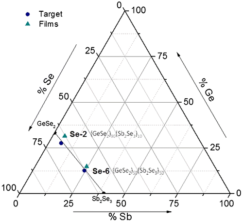
Figure 2. Chemical composition of (GeSe2)90(Sb2Se3)10 (Ge28.1Sb6.3Se65.6, Se2) and (GeSe2)50(Sb2Se3)50 (Ge12.5Sb25Se62.5, Se6) sputtered films and bulk glass targets determined by EDS analysis (±1 at.%) compared to theoretical composition.
Figures and indicate the dispersion of refractive index values in near- and mid-IR (6·3 and 7·7 μm) of the targets and corresponding RF sputtered thin films used for performing computer simulations based on the Effective Index Method.
Figure 3. Refractive index in near- and mid-IR (±0·01) extracted from VASE data of bulk targets and sputtered (Ge28.1Sb6.3Se65.6, Se2) and (Ge12.5Sb25Se62.5, Se6) thin films.
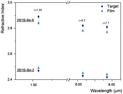
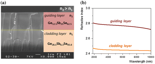
Figure 4. (a) SEM image of guiding (Ge12.5Sb25Se62.5, Se6) and cladding (Ge28.1Sb6.3Se65.6, Se2) sputtered layer of mid-IR structure, (b) dispersion curves of refractive indices (±0·01) of the sputtered layers, estimated by the analysis of VASE data via Sellmeier model.
Optical losses
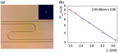
The optical losses were determining considering RF sputtered thin films presenting surface RMS roughness lower than 1 nm. Ridge selenide waveguides, with width from 8 to 14 μm and height about 1·7 μm, were obtained on Si substrate (Figure ). Spiral ridge, Y-junction and S-shape waveguides were also fabricated and optically characterized to evaluate the optical losses at 7·7 μm (Figure ). The widths of these transducers were 10, 12 and 14 μm. The simulation indicates negligible bending loss in selenide ridge waveguides whatever their widths for radius of curvature higher than 6 μm and the resulting optical loss is due to intrinsic propagation losses [Citation19]. The waveguide loss for single mode chalcogenide waveguides was measured using a cut back method from S-shape waveguides by using two guiding structure widths of 10 and 14 μm. The selenide ridge S-shape waveguides have propagation losses in the range of 2·5 ± 0·08 and 2·6 ± 0·06 dB cm−1 for waveguides of width 10 and 14 μm, respectively. The losses are related to the defects located at selenide layers interface and at the side wall roughness and volume scattering of selenide guiding layer. The waveguide losses are comparable to the values obtained in other mid-IR waveguide platform reported in silicon and germanium waveguides in this wavelength range (1–3 dB cm−1) and sufficiently low for sensor applications.
Figure 5. (a) Scheme and (b) SEM image of cross-section of chalcogenide ridge waveguide, (c) fundamental mode TM00 intensity profile for the optimal geometrical parameters (width w and height h) of chalcogenide waveguide and evolution of the evanescent power factor η as a function of w, h for single-mode propagation in the detection of any substance dissolved at λ = 7·66 μm.
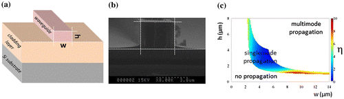
Figure 6. (a) Near field of propagated light at λ = 7·7 μm and microscopic image of single-mode ridge waveguides in S-shape configuration. (b) Optical propagation loss at λ = 7·7 μm measured by mode profile imaging method for selenide ridge waveguides with height equal to 1·7 μm and width of 10 μm. Each point represents averaged data for 3 experimental measures.
Chalcogenide functionalization by a polymer
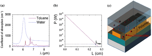
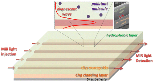
One of the major challenges for the detection of pollutant molecules is the strong absorbance and interference of water in the IR range. The detection of pollutant molecules by mid-IR-ATR spectroscopy requires surface functionalization by a hydrophobic film as the detection of aromatic hydrocarbons for instance, even for high concentration, is quite difficult in water. A polymeric membrane is used to extract pollutant molecules from water and also to decrease the water amount along the IR beam. Different materials were studied for their ability to extract molecules: Teflon AF2400, Poly(acrylonitrile-co-butadiene) (PAB), Polydimethylsiloxane (PDMS), Ethylene-propylene copolymer (EPco) and Polyisobutylene (PIB) [Citation24,25]. PIB is commonly used for its ability to extract small aromatic hydrocarbons such as BTX (benzene, toluene and xylenes). In this work, PIB was chosen as material for the functionalization of ZnSe prism and Ge–Sb–Se planar waveguide deposited on ZnSe prism surface in order to detect BTX in water (Figure ). The thickness of polymer film of about 4–5 μm was determined to obtain maximum attenuation of water absorbance while maintaining a pollutant diffusion speed through the polymer layer compatible with on-site analysis. The compatibility of PIB with the selenide waveguide was confirmed (Figure ).
Figure 7. (a) Mid-IR absorbance spectra of toluene at 100 v/v % and water at T = 278 K. (b) Power transmitted response as a function of the waveguide length taking into consideration the strong absorbance of water in the mid-IR. (c) Scheme of waveguide functionalization: a polymer non-absorbing in the mid-IR is deposited as superstrate for detection of pollutants dissolved in water.
Detection of substances in water environment
In order to guarantee the feasibility of detection of pollutants dissolved in water, an analysis of optical attenuation caused by the water absorption in the mid-IR as a function of the waveguide length is required (Figure (b)). Although the method is perfectly generalizable, the calculation was focused on the absorption peak of one of the BTX, the toluene at λ = 6·68 μm (Figure ). For this calculation, an evanescent power factor of η = 9% (from Figure (c)), an intrinsic propagation loss αprop = 1 dB cm−1 (this value is reachable by the manufacture optimization of the mid-IR selenide waveguide), a concentration of water Cwater = 5·50 mol L−1 = 100%v/v and molar absorption coefficient of water εwater = 11·38 mol−1 L cm−1 at λ = 6·68 μm were taken into consideration. The Lmax = 2·5 mm is obtained as the waveguide length which causes an attenuation of output power equivalent of the lowest optical signal, hence for detection of pollutant substances in water environments a ridge waveguide shorter than Lmax must be fabricated. Moreover, the optimum waveguide length for detection in aquatic media is estimated to be Lopt_aq = 176 μm. The minimum concentration of toluene dissolved in water at λ = 6·68 is calculated and Cmin_toluene = 6·20 × 10−5 mol L−1 = 5·7 ppm is obtained. This calculation considers a molar absorption of toluene equal to εtoluene = 97·4 mol−1 L cm−1. A high concentration of water is considered Cwater = 55·4945 mol L−1 = 99·99%v/v, the complementary parameters such as Lopt_aq = 176 μm. Even when Cmin_toluene is lower than the solubility threshold value, this result is not enough to consider this sensor as a threshold alarm tool because its limit of detection (LOD) is higher than the maximum contaminant level in drinking water. Therefore a second design for a sensor detecting in aquatic environments is presented; the LOD could be enhanced by functionalizing the superstrate of waveguide. The concept enables to limit the water absorption in the mid-IR by replacing water in contact with the surface of the chalcogenide waveguide by an optically non-absorbing material, particularly by a polymer like PIB, which is an hydrophobic polymer with a high transmittance in this range of wavelengths. The waveguide structure optimization takes advantage of permeability of the polymer to trap the molecules of pollutant substance while the water cannot circulate in this environment, as it is shown in the Figures (c) and . Moreover, the diffusion into the PIB leads to an accumulation effect of the solute molecules in vicinity of the evanescent field increasing the sensor performance. Thus, the expected minimum detectable concentration of toluene dissolved in water by using the polymer functionalization is Cmin_toluene PIB = 2·8345 × 10−7 mol L−1 = 26 ppb and the optimal length of waveguide for an optical non-absorbing medium Lopt = 4·3 cm. This result is noticeably lower than the maximum level of concentrations suggested by the international standards of quality of water and the mid-IR sensor could be exploited as an efficient monitoring tool.
Figure 8. Scheme of a mid-IR sensor constituted of a selenide buffer (Ge28.1Sb6.3Se65.6, Se2) and a ridge selenide waveguide (Ge12.5Sb25Se62.5, Se6) coated with a polymer allowing molecules detection by evanescent wave spectroscopy.
Conclusion
To conclude, mid-IR sensor based on a cladding Ge28.1Sb6.3Se65.6 layer and a guiding Ge12.5Sb25Se62.5 layer exploiting RF magnetron sputtering and RIE-ICP dry etching process was profitably designed and fabricated. Waveguide losses were measured to be ~2·5 dB cm−1 at 7·7 μm. Then, the light injection efficiency experiments were carried out in mid-IR (7·7 μm) in Y-junction, spiral and S-shape waveguides; the light confinement was observed for all the designs. Finally, to detect pollutant molecules in water by the evanescent field, the waveguide surface was functionalized by depositing a polymer film by spin coating. As a result, we demonstrated the feasibility of chalcogenide waveguides fabrication for mid-IR detection of organic molecules in water. These technological, experimental and theoretical results represent a first step towards the development of an integrated optical sensor operating in the mid-IR wavelength range.
Disclosure statement
No potential conflict of interest was reported by the authors.
Funding
This work was financially supported by the Region Bretagne, IFREMER and BRGM through an interCarnot fund, LOUISE ANR project, and Czech Science Foundation [project number 16-17921S].
References
- Conmy RN, Coble PG, Farr J, et al. Submersible optical sensors exposed to chemically dispersed crude oil: wave tank simulations for improved oil spill monitoring. Environ Sci Technol. 2014;48:1803–1810.10.1021/es404206y
- Silverstein R, Webster F, Kiemle D, editors. Spectrometric identification of organic compounds. Hoboken, NJ: Wiley; 2005.
- Sieger M, Haas J, Jetter M, et al. Mid-infrared spectroscopy platform based on GaAs/AIGaAs thin-film waveguides and quantum cascade lasers. Anal Chem. 2016;88:2558–2562.10.1021/acs.analchem.5b04144
- Pejcic B, Eadington P, Ross A. Environmental monitoring of hydrocarbons: a chemical sensor perspective. Environ Sci Technol. 2007;41:6333–6342.10.1021/es0704535
- Kim SS, Young C, Mizaikoff B. Miniaturized mid-infrared sensor technologies. Anal Bioanal Chem. 2008;390:231–237.10.1007/s00216-007-1673-5
- Singh V, Lin PT, Patel N, et al. Mid-infrared materials and devices on a Si platform for optical sensing. Sci Technol Adv Mater. 2014;15:014603.
- Hu J, Gmachl C. SPECTROSCOPY QCL-based sensors target health and environmental applications. LFW. 2012;48:39–43.
- Soref R. Mid-infrared photonics in silicon and germanium. Nat Photon. 2010;4:495–497.10.1038/nphoton.2010.171
- Sieger M, Mizaikoff B. Toward on-chip mid-infrared sensors. Anal Chem. 2016;88:5562–5573.10.1021/acs.analchem.5b04143
- Ma P, Choi D-Y, Yu Y, et al. Low-loss chalcogenide waveguides for chemical sensing in the mid-infrared. Opt Express. 2013;21:29927–29937.10.1364/OE.21.029927
- Tsay C, Zha Y, Arnold CB. Solution-processed chalcogenide glass for integrated single-mode mid-infrared waveguides. Opt Express. 2010;18:26744–26753.10.1364/OE.18.026744
- Lin H, Li L, Deng F, et al. Demonstration of mid-infrared waveguide photonic crystal cavities. Opt Lett. 2013;38:2779–2782.10.1364/OL.38.002779
- Ma P, Choi DY, Yu Y, et al. High Q factor chalcogenide ring resonators for cavity-enhanced MIR spectroscopic sensing. Opt Express. 2015;23:19969–19979.10.1364/OE.23.019969
- Anne ML, Keirsse J, Nazabal V, et al. Chalcogenide glass optical waveguides for infrared biosensing. Sensors. 2009;9:7398–7411.10.3390/s90907398
- Ganjoo A, Jain H, Yu C, et al. Detection and fingerprinting of pathogens: mid-IR biosensor using amorphous chalcogenide films. J Non-Cryst Solids. 2008;354:2757–2762.10.1016/j.jnoncrysol.2007.09.095
- Verger F, Nazabal V, Colas F, et al. RF sputtered amorphous chalcogenide thin films for surface enhanced infrared absorption spectroscopy. Opt Mater Express. 2013;3:2112–2131.10.1364/OME.3.002112
- Němec P, Olivier M, Baudet E, et al. Optical properties of (GeSe2)100−x(Sb2Se3)x glasses in near- and middle-infrared spectral regions. Mater Res Bull. 2014;51:176–179.10.1016/j.materresbull.2013.11.050
- Baudet E, Gutierrez-Arroyo A, Němec P, et al. Selenide sputtered films development for MIR environmental sensor. Opt Mater Express. 2016;6:2616–2627.10.1364/OME.6.002616
- Gutierrez-Arroyo A, Baudet E, Bodiou L, et al. Optical characterization at 7.7 μm of an integrated platform based on chalcogenide waveguides for sensing applications in the mid-infrared. Opt Express. 2016;24:23109–23117.10.1364/OE.24.023109
- Gutierrez-Arroyo A, Baudet E, Bodiou L, et al. Theoretical study of an evanescent optical integrated sensor for multipurpose detection of gases and liquids in the mid-infrared. Sens Actuators B-Chem. 2017;242:842–848.
- Siebert R, Muller J. Infrared integrated optical evanescent field sensor for gas analysis part I: system design. Sens Actuators A-Phys. 2005;119:138–149.10.1016/j.sna.2004.11.001
- Charrier J, Brandily ML, Lhermite H, et al. Evanescent wave optical micro-sensor based on chalcogenide glass. Sens Actuators B-Chem. 2012;173:468–476.10.1016/j.snb.2012.07.056
- Mattox DM, editor. Handbook of physical vapor deposition (PVD) processing. Norwich, NY: Elsevier; 2010.
- Pejcic B, Boyd L, Myers M, et al. Direct quantification of aromatic hydrocarbons in geochemical fluids with a mid-infrared attenuated total reflection sensor. Org Geochem. 2013;55:63–71.10.1016/j.orggeochem.2012.11.011
- Flavin K, Hughes H, Dobbyn V, et al. A comparison of polymeric materials as pre-concentrating media for use with ATR/FTIR sensing. Int J Environ Anal Chem. 2006;86:401–415.10.1080/03067310500291585