
Abstract
Induced coupled plasma etching was performed on poly-crystalline boron-doped diamond (BDD) films synthesized by microwave assisted chemical vapor deposition (MWCVD). Effects of the input power and of the gas composition and pressure on etching performances have been investigated. A basic aluminium layer and a new hybrid material have been studied as protecting film for the patterning. Best conditions to get high etch rates were a gas ratio Ar/O2 of 27% (vol.) under 10 mTorr at 200 W (input power). Aluminium (Al) masking induced un-intentional whiskers formation which was removable using CHF3 as a reactive gas with the drawback to lower the process selectivity. In order to get both a high etching rate and a high selectivity, a hybrid material based on an organic/mineral resin was then used as the masking material. This performing photoresist film allowed etching a 3.6-μm-thick BDD film at 200 nm min−1.
1. Introduction
Microfabrication technologies have drawn considerable interest in the field of fabrication of electrodes for electrochemical sensors especially because of the facility of low-cost mass production with a well-defined patterning. In the aim to build a micro total analysis system devoted to the detection of heavy metals ions, all components (i.e. detection and microfluidic) have to be integrated on a lab-on-a-chip device. Very sensitive electrochemical microsensors with mercury (Hg) [Citation1–3] or bismuth [Citation4] working electrodes have been developed for the detection of heavy metals with very low detection limit. However, the toxicity of Hg and the stability of bismuth are needed to develop new materials for electrochemical sensing. A boron-doped diamond (BDD) has been recently proposed for this purpose because of its great electrochemical properties toward especially heavy metals reduction.[Citation5] In this way, Madore et al. [Citation6] have synthesized BDD films by microwave plasma-assisted chemical vapor deposition (CVD) and patterned the material by photolithography: an Si3N4 layer was then deposited and etched to produce a hexagonal array of 5 μm diameter BDD microdisks spaced to 100 μm. Tsunozaki et al. [Citation7] have used a photoresist film to prepare BDD tips. The first stage was an isotropic etching of a Si surface followed by a deposition of BDD, a spin-coating and hence a mechanical etching of a polyimide film to prepare the tips array (tips size 25–30 μm in diameter). The as-prepared diamond microelectrodes array showed a great interest in electroanalysis. More recently Pagels et al. [Citation8] have prepared an original microsystem constituted of a hexagonal BDD microdisks array on an insulated diamond matrix. The main property being to obtain a coplanar system instead of an array made of BDD wells or tips.
Despite the numerous works devoted to BDD for sensing applications, from the best of our knowledge, BDD arrays devoted to electrochemical measurements have never been directly integrated on a unique substrate constituting the working electrode, the counter electrode and the reference electrode. For this purpose, an efficient method of BDD etching has to be developed to get a well-patterned film.
For a deep and clean removal and patterning of a diamond-like material not only a sufficient etching rate but also an adequate selectivity of the applied process relative to the masking layer is required. Therefore, different masks were tested here and several etching conditions were studied referring to their applicability to the removal of BDD.
Reactive ionic etching (RIE) comprises two related mechanisms: chemical reactive etching and physical sputtering etching. The former leads to a high etch rate but is isotropic whereas the latter leads to a lower etch rate but is anisotropic. In the gas mixture Ar/O2, Ar (as the inert gas) induces the physical sputtering etching and oxygen as the reactive gas the chemical ion-enhanced etching. The way to realize high-quality patterning (i.e. high aspect ratio and/or high etching rate) is to control the proportion of these two factors. Main parameters are the Ar/O2 ratio, the radiofrequency (RF) power, the gas pressure, the presence of a reactive gas as CHF3 and the choice of the mask.
In the present work, we have studied the effect of the physical and chemical conditions on the etching rate and on the surface aspect of BDD films.
2. Experimental
2.1. BDD film synthesis
The poly-crystalline BBD films were grown by plasma-assisted CVD in a bell-jar reactor (PLASSYS BJS 150) previously described in [Citation9]. An <100> oriented silicon wafer (2″ in diameter and 1 mm thick) was used as a substrate. The wafer was treated in an ultrasonic bath with a diamond grit to promote a surface seeding and then the diamond nucleation. High-purity methane and diborane diluted in hydrogen were used as the gas mixture. The (B/C) ratio in the gas phase and the methane concentration were set at 1000 ppm and 4%, respectively. The total pressure was set at 180 mbar, the input microwave power at 3 kW for 2 h and the substrate temperature at 850°C. These conditions are suitable for high-quality diamond growth with relatively high growth rates. The as-prepared boron diamond film had a thickness of 3.6 μm. The conductivity and the charge carrier density (determined by the four probes method associated with the Hall effect (donner le nom de l'appareil)) were 563±73 S cm−1 and cm−3, respectively. The charge carrier density is superior to the metallic transition (
cm−3) which proved the high doping of the structure.
2.2. Sample preparation for etching experiments
2.2.1. Al mask
About 25 mm2 BDD samples were first washed with acetone and ultrapure water and dried under nitrogen. A part of the area was then coated by an organic resin (Picéine®). The Al mask was deposited on the whole surface by thermal evaporation at 500°C and 10−6 mbar using a current of 100 A. The Al deposit rate was 15 Å s−1 and the time deposit was 3 min (i.e. mask thickness was 270 nm). The next step was the dissolution of the Picéine® resin by immersion in trichloroethylene for 30 s to get samples constituting of BDD and Al separated by a 270 nm high step (Al layer thickness). Before etching, samples were washed in ultrapure water and acetone (twice). Finally to recover a full BDD surface after etching, the Al mask was dissolved for 10 min in the following acid mixture (vol/vol), washed in ultrapure water and dried under nitrogen.
2.2.2. Hybrid resin-based mask
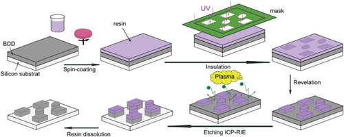
The stages of the deposit of the hybrid mask and the etching are depicted in . The first step was the spin-coating (1200 rpm for 30 s, spin-coater DELTA 10BM) of the negative resin (K-CL® type, KLOE France). The resin was a methacrylate/siloxane hybrid material prepared by sol–gel and used as bought. After spin-coating, samples were dried at 80°C for 10 min to get an optimal adhesion on the BDD surface. Samples were then insulated at 365 nm for 90 s and immersed in isobutanol (90 s) for the liftoff. After etching, the mineral mask was removed by dissolution in acetone and methanol.
Figure 1. Description of the etching process of the BDD film based on the use of a hybrid organic/mineral photoresist mask.
2.3. Etching method and condition
The RIE experiments were performed using an induced coupled plasma (ICP) etcher Corial 200IL (using a 800 W and 2 MHz ICP source) with RF excitation at 13.56 MHz adjustable from 50 to 300 W. The cathode was 22 cm in diameter and was continuously cooled with a helium flow. The pressure in the chamber was maintained by a turbomolecular magnetic pump (ATH 500 Alcatel). Prior to each experiment, the electronic grade gases of either Ar/O2 or CHF3/O2 were introduced into the reaction chamber through a gas box by means of gas controllers. The compositions examined were a ratio Ar/O2 from 5/40 to 30/40 and a ratio CHF3/O2 of 5/40 (sccm/sccm).
The etch depth of the BDD film was measured using a DEKTAK 3 stylus profilometer with an average of three scans performed after each experiments. In addition, a selection of features on the surfaces was examined by scanning electron microscopy (SEM) (Cambridge 200) and whiskers density was determined by image analysis using the software IMAGE J.
3. Results and discussions
3.1. BDD etching patterned by an Al mask
3.1.1. Ar/O2 ratio effect
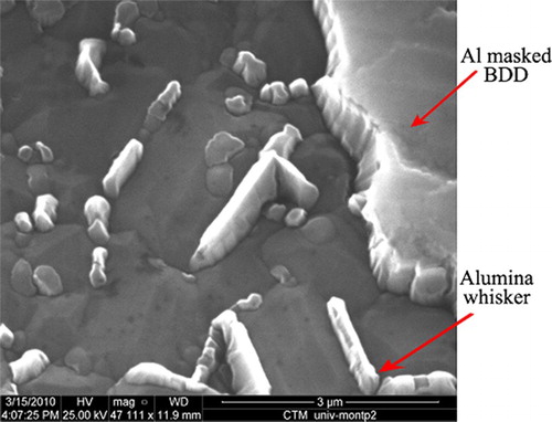
In this part the RF power at 13.56 MHz was 100 W, etching time 10 min and the working pressure 10 mTorr. shows the surface morphology of the etched BDD at a ratio (sccm/sccm). The deposits (called whiskers) identified at the grain boundaries of the etched diamond surface are due to Al sputtering. Indeed during the etching process, Al atoms are ionized in Al(III) ions which reacted with the oxygen plasma to form Al2O3 crystals, identified by energy dispersive X-ray.
Figure 2. SEM image of a BDD film etched at 10 mTorr with a ratio Ar/O2=5/40 (sccm/sccm) and a RF power 100 W.
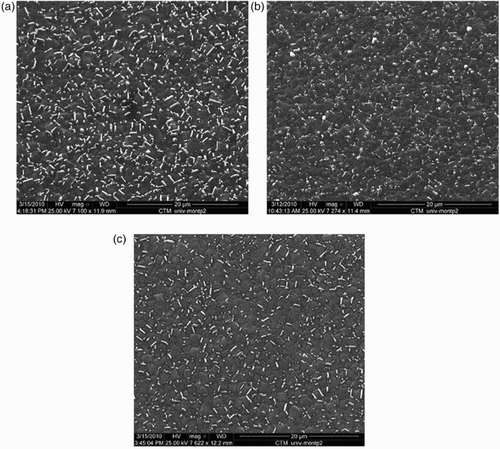
shows the surface of the BDD samples etched at different argon contents. The whiskers density was determined by image analysis (Image J® software). The micromask densities were 12%, 9% and 7% of the analysed area for samples etched with 11%, 27% and 43% of Ar in the mixture, respectively, which proved that Al sputtering and Al2O3 deposition were mainly due to oxygen chemical etching.
Figure 3. SEM images of a BDD film etched at 10 mTorr and 100 W with (a) Ar=11% vol. (ratio Ar/O2=5/40), (b) Ar=27% vol. (ratio Ar/O2=15/40) and (c) Ar=43% vol. (ratio Ar/O2=30/40 (sccm/sccm)).
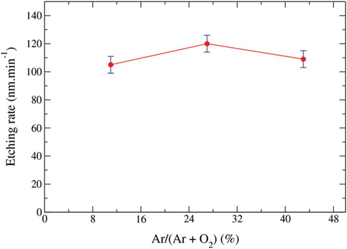
Moreover, the etching rates of BDD by Ar/O2 plasma are shown in . The highest etching rate (120 nm min−1) is obtained for an Ar content in the plasma of 27%. RIE of the diamond in Ar-based mixtures was studied by Leech and Reeves.[Citation10] Authors determined high (30 nm min−1) and low-rate (7–10 nm min−1) regimes for ratios
and
, respectively. Both regimes were identified as ion-enhanced chemical etching and physical sputtering, respectively. The high etching rates observed in our cases for BDD were then linked to the use of high oxygen contents in the mixture (i.e. >57% of O2) in accordance with Leech's results. In pure oxygen plasmas, the etching has been attributed to a dissociation of oxygen into O radicals [Citation11] accompanied by the formation of volatile etch products of CO and CO2. For diamond etching, pure O2 plasmas were much more reactive than pure Ar plasmas (28 nm min−1 and 8 nm min−1, respectively [Citation10]). As observed from for a value of argon superior to 27% in the mixture, an increase in the Ar content led to a decrease in the etching rate. We assume that for Ar values lower than 27%, physical sputtering was negligible compared to chemical etching and that the high oxygen content led to a high micromask density () which acted as a protected layer for the BDD surface and then induced lower etch rates. The best conditions to get both a high rate regime and a low whiskers density were then a ratio
of 27% for a RF power of 100 W and a pressure of 10 mTorr.
Figure 4. Effect of Ar content on the etch rate of the BDD film. O2 flux 40 sccm, RF power 100 W, pressure 10 mTorr, and etching time 10 min.
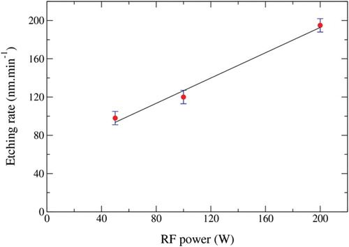
3.1.2. RF power effect
shows the etching rate as the function of the RF power in the range 50–200 W for a chamber pressure of 10 mTorr. The etching rate increased linearly with increase in the RF power which indicated that the production of energetic oxygen species was also increasing as well as the bond breaking efficiency.[Citation12,Citation13]
Figure 5. Effect of the RF power on the etch rate of the BDD film. Ar/O2=15/40 (sccm/sccm), pressure 10 mTorr and etching time 10 min.
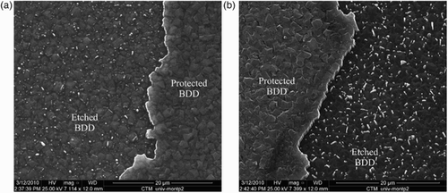
Micrographies of show that the whiskers density increased with the RF power. As for a constant Ar/O2 ratio, a power increase led to a higher increase in the chemical etching due to oxygen than of the physical sputtering due to argon, whiskers formation was then mainly related to chemical etching.
Figure 6. SEM images of the etched film with Ar/O2 15/40 (sccm/sccm), pressure 10 mTorr, etching time 10 min and RF power 100 W (a) and 200 W (b).
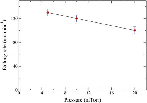
3.1.3. Gas pressure dependence
The influence of process pressure on the etch rate is depicted in for a ratio Ar/O2 of 15/40 (sccm/sccm) and a RF power of 100 W. The higher etch rate was obtained at 5 mTorr (130 nm min−1). For higher pressure, a decrease in the etch rate was recorded because of the enhanced ion–ion and ion-electron recombinations which decreased the quantity of accelerated ions with sufficient energy for material removal. The whiskers’ densities were also determined at 5, 10 and 20 mTorr and were 8.8%, 9% and 13.8%, respectively. We have previously shown that alumina whiskers formation was related to a high degree of chemical etching. Then as the whiskers density remained high despite a low etching rate, the decrease in the etch rate could be mainly due to a lowering of the physical sputtering due to Ar ions recombination as proposed by Jiang et al.[Citation14]
Figure 7. Effect of the pressure on the etching rate of BDD film (Ar/O2 15/40 (sccm/sccm), etching time 10 min and an RF power 100 W).
3.1.4. CHF3 effect
Fluorocompounds are commonly used in the etching process because of the positive effect on the etch rate of the fluorine radical.[Citation15] The use of a mixture CHF3/O2 is particularly of interest to enhance the etch rate. Indeed the concentration of fluorine atoms responsible for the etching is increased by the enhanced dissociation of C‒ F bonds through reacting with oxygen atoms.[Citation16,Citation17] Unfortunately, the drawback is a decrease in etching selectivity. In this way, Ando et al. [Citation18] have proved that the increase in CF4/O2 ratio reduced the selective etching ratio of diamond against Al.
A ratio (sccm/sccm) led to a etch rate of the BDD film of 130 nm min−1 for a pressure of 10 mTorr, an RF power of 200 W and an etching time of 10 min. Such conditions allowed etching without whiskers as proved by the micrography of the surface shown in . Note that during the 10-min-etching process, the entire Al mask (i.e. 250 nm) was removed which shows the poor selectivity of the CHF3/O2-based etching process (lower that 5) compared with the process carried out in the mixture Ar/O2 for which the selectivity was from 5–10 (i.e. etching rate from 100 to 200 nm min−1). The determined value of 130 nm min−1 was then given by default because of the entire removal of Al and the slight etching of the no more protected BDD surface.
Figure 8. SEM image of the etched film with CHF3/O2 5/40 (sccm/sccm), pressure 10 mTorr, etching time 10 min and an RF power 200 W.
The absence of alumina whiskers could be related to both phenomena. First, hydrogen atoms derived from the dissociation of CHF3 reacted with Al to produce alane (AlH3) which are volatile products.[Citation19,Citation20] Second, the presence of CHF3 could also remove more efficiently the deposited alumina than pure O2 (by chemical etching) or than Ar (by physical sputtering).
CHF3 seems then to be a good candidate to etch BDD but with the drawback to decrease the selectivity against BDD face to Al which is unacceptable to pattern thick diamond layers.
Finally very high etching rates (i.e. 200 nm min−1) of BDD were obtained by controlling the input power, the pressure, the nature of the etching gas and their ratio. Nevertheless, whatever were the conditions in the presence of argon, alumina whiskers were identified at the grains boundaries of the films. Contamination of the surface is definitely excluded for MEMS applications and especially in the aim to use the patterned films as the active layer of an electrochemical sensor. The only way to get a sample free of whiskers was to use the mixture CHF3/O2. But this gas mixture induced a high etch rate of Al mask and then a poor process selectivity. Then it was necessary to develop a new kind of mask as presented in the following section.
3.2. BDD etching patterned by a hybrid resin
Most of the studies devoted to the etching of diamond-like materials are based on the use of metals or metallic alloys as masking materials. Very few works in the field used photoresist films to pattern the diamond especially because of the very low resistance of most of the organic-based resins against RIE. To develop an alternative to metallic masks to get both a high selectivity and a high etch rate of BDD without metallic oxides whiskers deposition, a new hybrid resin was investigated here. The resin was synthesized by the sol–gel method from organo-mineral precursors to get a hybrid material in which the organic groups confer the photosensitive properties, while the mineral portion contributes to the mechanical and thermal stability and to the resistance against etching. We did not want to use fluorocompounds as the reactive gas to develop a process as simple as possible. Then the experimental conditions tested were the followings: ratio Ar/O2 15/40 (sccm/sccm), pressure 10 mTorr and RF power 200 W because the etch rate determined in these conditions was the highest (195 nm min−1). The initial thickness of the protecting layer was 8.5 μm.
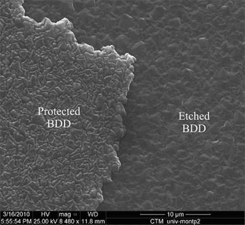
Different views obtained by SEM of the etched BDD film before and after dissolution of the protective hybrid layer are shown in .
Figure 9. SEM images of different areas of the BDD film etched under a flux of Ar/O2 15/40 (sccm/sccm), at 10 mTorr with an RF power of 200 W (a) before and (b) after resin dissolution. The thicknesses of the BDD film and of the resin layer are 3.6 and 8.5 μm, respectively.
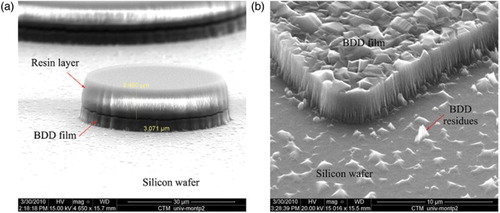
The etching rate of the BDD film, determined after 10 min etching, was 200 nm min−1 in accordance with the previous results obtained with the Al mask. As predicted no whiskers were identified on the etched surface. After 18 min of processing, the entire BDD film was removed without the hybrid protective layer etching as depicted in . Results show the very high selectivity of the process using the new hybrid mask compared with the Al one for which the selectivity is lower than 10 as previously proved.
4. Conclusion
BDD was successfully etched by ICP-RIE with a high etch rate. The etch rate increased with higher RF power and lower gas pressure and depended also on the gas ratio Ar/O2. The etch rate decrease with gas pressure increase was related to Ar ions recombination. Best conditions to get the highest etch rate (i.e. 195–200 nm min−1) was a ratio Ar/O2 of 15/40 (sccm/sccm) (i.e. 27 % of Ar in the mixture), an RF power of 200 W and a pressure of 10 mTorr. Two types of masking were investigated. Basic Al masks induced the formation of alumina whiskers located at the grain boundaries of the polycrystalline BDD film. The whiskers’ surface density decreased with increasing Ar content and the formation was mainly related to oxygen chemical etching of the Al mask. The gas mixture CHF3/O2 led to an etched surface free of alumina whiskers because of the formation of volatile alane (AlH3) with the drawback of a very low process selectivity (inferior to 5) which is unacceptable to pattern the thick diamond film. Finally, we have proposed a new commercial hybrid organic/mineral resin to pattern BDD without whiskers formation at a high etching rate (200 nm min−1) and selectivity. In the optimal conditions, a BDD layer of 3.6 μm thick was then etched in 18 min without any removal of the 8.5-μm-thick hybrid protective layer.
References
- Reay RJ, Flannery AF, Storment CW, Kounaves SP, Kovacs GTA. Microfabricated electrochemical analysis system for heavy metal detection. Sens Actuat B: Chem. 1996;34:450–455. doi: 10.1016/S0925-4005(97)80018-4
- Choi JY, Seo K, Cho SR, Oh JR, Kahng SH, Park J. Screen-printed anodic stripping voltammetric sensor containing HgO for heavy metal analysis. Anal Chim Acta. 2001;443:241–247. doi: 10.1016/S0003-2670(01)01219-3
- Zhu X, Gao C, Choi JW, Bishop PL, Ahn CH. On-chip generated mercury microelectrode for heavy metal ion detection. Lab Chip. 2005;5:212–217. doi: 10.1039/b410006a
- Zou Z, Jang A, MacKnight E, Wu PM, Do J, Bishop PL, Ahn CH. Environmentally friendly disposable sensors with microfabricated on-chip planar bismuth electrode for in situ heavy metal ions measurement. Sens Actuat B Chem. 2008;134:18–24. doi: 10.1016/j.snb.2008.04.005
- McGaw EA, Swain GM. A comparison of boron-doped diamond thin-film and Hg-coated glassy carbon electrodes for anodic stripping voltammetric determination of heavy metal ions in aqueous media. Anal Chim Acta. 2006;575: 180–189. doi: 10.1016/j.aca.2006.05.094
- Madore C, Duret A, Haenni W, Perret A. Microfabricated systems and MEMS V: detection of trace silver and copper at an array of boron-doped diamond microdisk electrodes. New Jersey, NJ: The Elctrochemical Society; 2000. p. 159–168.
- Tsunozaki K, Einaga Y, Rao TN, Fujishima A. Fabrication and electrochemical characterization of boron-doped diamond microdisc array electrodes. Chem Lett. 2002;5:502–503. doi: 10.1246/cl.2002.502
- Pagels M, Hall CE, Lawrence NS, Meredith A, Jones TGJ, Godfried HP, Pickles CSJ, Wilman J, Banks CE, Compton RG, Jiang L. All-diamond microelectrode array device. Anal Chem. 2005;77:3705–3708. doi: 10.1021/ac0502100
- Silva F, Hassouni K, Bonnin X, Gicquel A. Microwave engineering of plasma-assisted CVD reactors for diamond deposition. J Phys: Condens Matter. 2009;21:364202-1–364202-16.
- Leech PW, Reeves GK, Holland AS. Reactive ion etching of diamond in CF4, O2, O2 and Ar mixtures. J Mater Sci. 2001;36:3453–3459. doi: 10.1023/A:1017964129419
- Williams KR, Muller RS. Etch rates for micromachining processing. J Microelectromechanical Syst. 1996;5(4): 256–269. doi: 10.1109/84.546406
- Lee JM, Chang KM, Kim SW, Huh C, Lee IH, Park SJ. Dry etch damage in n-type GaN and its recovery by treatment with an N2 plasma. J Appl Phys. 2000;87:7667–7670. doi: 10.1063/1.373438
- Feng MS, Guo JD, Lu YM, Chang EY. Reactive ion etching of GaN with BCL3/SF6 plasmas. Mater Chem Phys. 1996;45:80–83. doi: 10.1016/0254-0584(96)80053-8
- Jiang L, Plank NOV, Blauw MA, Cheung R, Drift EVD. Dry etching of SiC in inductively coupled Cl2/Ar plasma. J Phys D: Appl Phys. 2004;37:1809–1814. doi: 10.1088/0022-3727/37/13/012
- Kuo Y. Plasma swelling of photoresist. Jpn J Appl Phys. 1993;32:L126–L128. doi: 10.1143/JJAP.32.L126
- Lanois F, Planson D, Locatelli M-L, Lassagne P, Jaussaud C, Chante J-P. Chemical contribution of oxygen to silicon carbide plasma etching kinetics in a distributed electron cyclotron resonance (DECR) reactor. J Electron Mater. 1999;28:219–224. doi: 10.1007/s11664-999-0017-y
- Khan FA, Adesida I. High rate etching of SiC using inductively coupled plasma reactive ion etching in SF6-based gas mixtures. Appl Phys Lett. 1999;75:2268–2270. doi: 10.1063/1.124986
- Ando Y, Nishibayashi Y, Kobashi K, Hirao T, Oura K. Smooth and high-rate reactive ion etching of diamond. Diam Relat Mat. 2002;11:824–827. doi: 10.1016/S0925-9635(01)00617-3
- Pan WS, Steckl AJ. Reactive ion etching of SiC thin films by mixtures of fluorinated gases and oxygen. J Electrochem Soc. 1990;137:212–220. doi: 10.1149/1.2086368
- Yih PH, Saxena V, Steckl AJ. A review of SiC reactive ion etching in fluorinated plasmas. Phys Status Solidi B. 1997;202:605–642. doi: 10.1002/1521-3951(199707)202:1<605::AID-PSSB605>3.0.CO;2-Y